Method for growing high-resistance N type epitaxial layer on heavily-doped P type substrate

A heavily doped, epitaxial layer technology, applied in electrical components, semiconductor/solid-state device manufacturing, circuits, etc., can solve the problems of reduced machine utilization, inability to mass production, long time consumption, etc., to achieve stable and controllable resistivity , Eliminate self-doping effect, uniform thickness effect

Inactive Publication Date: 2012-01-18
ADVANCED SEMICON MFG CO LTD
View PDF9 Cites 10 Cited by
  • Summary
  • Abstract
  • Description
  • Claims
  • Application Information

AI Technical Summary

Problems solved by technology

Due to the reverse expansion of the heavily doped P-type substrate during the epitaxial growth process and the self-doping effect of the process chamber itself, the influence of impurities adsorbed on the gas tube wall after idle, etc., to obtain a uniformly doped N-type epitaxy has a great impact on the process. It is extremely challenging, especially the repeatability between wafers
[0003] The current status quo is: due to the different degrees of P-type self-doping, the process conversion between different substrates and products takes a long time, and the same program cannot satisfy all products.
Due to the unstable process, the success rate of the mass-produced 0.014-0.020 ohm cm substrate expansion resistor is low, resulting in a decrease in the utilization rate of the machine
In addition, N-type high-resistance epitaxy on a P-type substrate of 0.009-0.013 ohm-cm and a substrate of 0.0025-0.004 ohm-cm cannot obtain good extended resistance patterns, and cannot be mass-produced on 8-inch lines.

Method used


Image

  • Method for growing high-resistance N type epitaxial layer on heavily-doped P type substrate
  • Method for growing high-resistance N type epitaxial layer on heavily-doped P type substrate
  • Method for growing high-resistance N type epitaxial layer on heavily-doped P type substrate

Examples


Embodiment Construction

[0026] The present invention will be further described below in conjunction with specific embodiment and accompanying drawing, set forth more details in the following description so as to fully understand the present invention, but the present invention can obviously be implemented in a variety of other ways different from this description, Those skilled in the art can make similar promotions and deductions based on actual application situations without violating the connotation of the present invention, so the content of this specific embodiment should not limit the protection scope of the present invention.

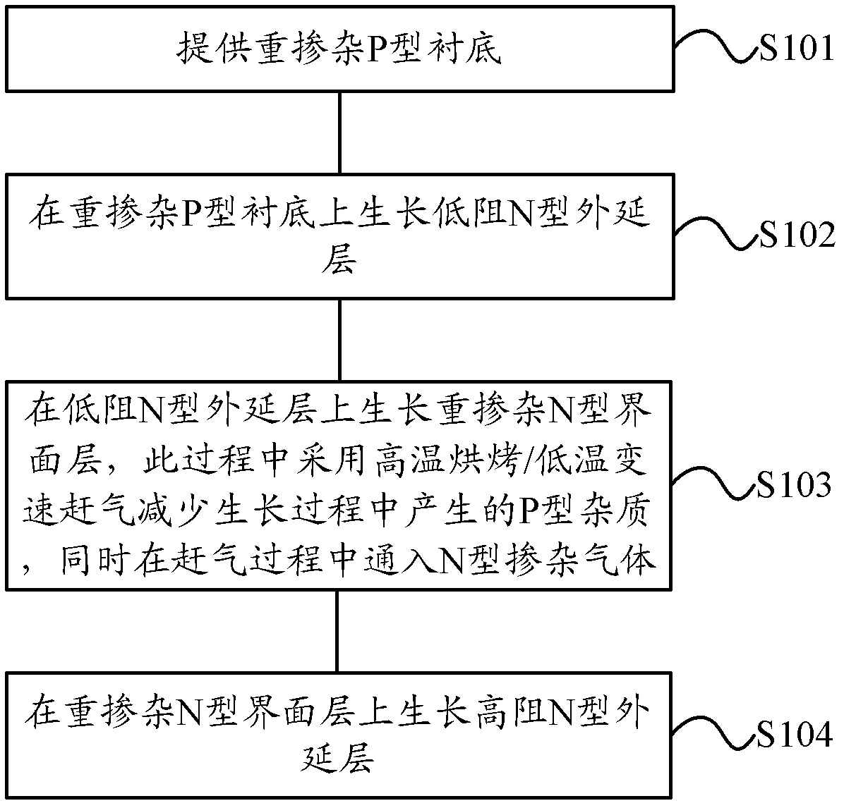
[0027] figure 1 It is a flowchart of a method for growing a high-resistance N-type epitaxial layer on a heavily doped P-type substrate according to an embodiment of the present invention. As shown, the method may include:

[0028] Execute step S101 to provide a heavily doped P-type substrate;

[0029] Executing step S102, growing a low-resistance N-type epitaxial laye...


PUM


Abstract

The invention provides a method for growing a high-resistance N type epitaxial layer on a heavily-doped P type substrate. The method comprises the following steps of: A, providing the heavily-doped P type substrate; B, growing a low-resistance N type epitaxial layer on the heavily-doped P type substrate; C, growing a heavily-doped N type interface layer on the low-resistance N type epitaxial layer, wherein high-temperature baking/low-temperature variable-speed gas driving is adopted to reduce P type impurities generated in the growing process, and simultaneously an N type doped gas is introduced in the process of gas driving; and D, growing the high-resistance N type epitaxial layer on the heavily-doped N type interface layer. The high-resistance N type epitaxial layer is uniform in thickness, is stable and controllable in resistivity in an area within 10 mm from an edge, and has an ideal spreading resistance pattern (SRP) curve; moreover, the product yield reaches over 99 percent, and the mass production of the high-resistance N type epitaxial layer by using an 8-inch line can be realized.

Description

technical field [0001] The invention relates to the technical field of semiconductor manufacturing, in particular to a method for growing a high-resistance N-type epitaxial layer on a heavily doped P-type substrate. Background technique [0002] Ultra-low capacitance transient voltage suppressors (TVS) can be used to protect high-frequency circuits from transient voltage transitions and suppress surges. Its low capacitance period consists of a low breakdown voltage avalanche diode and a low capacitance steering diode. The biggest feature of the latter is that it grows a high-resistance N-type epitaxial layer (150-400 ohm-cm) on a heavily doped (heavily doped) P-type substrate (resistivity 0.009-0.013 ohm-cm) to form a super low capacitance diodes. In order to obtain a sufficiently low capacitance, the resistivity requirements for the high-resistance epitaxy are very strict, and it is required to be close to the epitaxy of this certificate (resistivity greater than 150 ohm ...

Claims


Application Information

Patent Timeline
Patent Type & Authority Applications(China)
IPC IPC(8): H01L21/20H01L21/329
Inventor 王海红史超何瑞徐雷军梁博
Owner ADVANCED SEMICON MFG CO LTD
Why Eureka
Try Eureka