Electronic device and optical sensing module thereof

A technology of sensing modules and electronic devices, which is applied in the input/output process of electrical digital data processing, instruments, and data processing, etc., can solve the problems of reducing comfort, difficulty in integration, and glare of light, so as to prevent glare and improve The effect of comfort

Inactive Publication Date: 2012-02-08
APEXONE MICROELECTRONICS SHANGHAI +1
View PDF2 Cites 6 Cited by
  • Summary
  • Abstract
  • Description
  • Claims
  • Application Information

AI Technical Summary

Problems solved by technology

[0002] Mouse, touchpad and trackball are the most commonly used human-machine interface devices, but the problems of these devices are that they are large in size and complex in structure, and are not easy to be integrated on portable electronic devices such as mobile phones and e-books
Although the optical indicating device disclosed in this patent can realize the predetermined function, the first disadvantage is that when the parallel light perpendicular to the transmission plane 114 is irradiated on the navigation panel 115, a part of the light is scattered on the navigation panel 115 through refraction. On the surface, it may cause glare and reduce the comfort of use. The second disadvantage is that the optical indicator module has many components, which is not conducive to reducing manufacturing costs. At the same time, the height is high, which is inconvenient to integrate on the increasingly thin and light portable electronic devices.

Method used


Image

  • Electronic device and optical sensing module thereof
  • Electronic device and optical sensing module thereof
  • Electronic device and optical sensing module thereof

Examples


Embodiment Construction

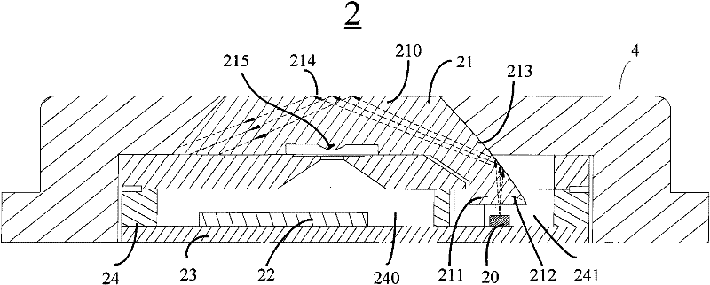
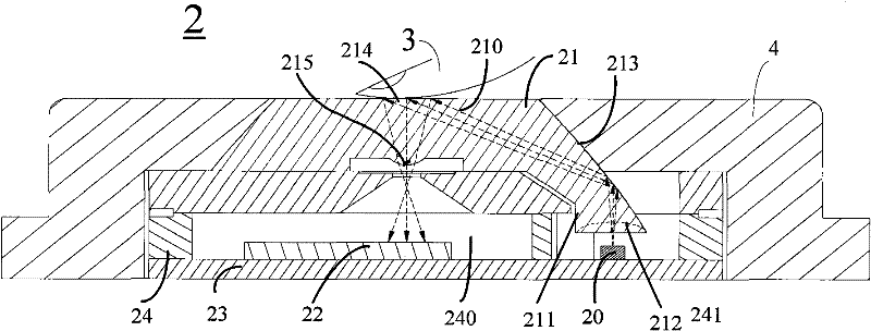
[0043] see figure 2 As shown, it is a schematic structural diagram of an optical sensing module implementing the present invention, wherein the optical sensing module 2 includes a light source 20 , a lens 21 , a photosensitive chip 22 and a circuit board 23 . Wherein the light source 20 and the photosensitive chip 22 are installed on the circuit board 23 and electrically connected with the circuit board 23 . In a specific implementation, the light source 20 may be a coherent light source (such as laser) or an incoherent light source. Preferably, the light source 20 is mounted on the circuit board 23 by surface-mounting technology. The circuit board 23 can be a printed circuit board or a flexible printed circuit board, and one end of the circuit board 23 is provided with an interface connected to the circuit board (not shown) of the circuit device using the optical sensing module 2, For example, gold fingers or electrical connectors are electrically connected to the main circ...


PUM


Abstract

The invention discloses an electronic device and an optical sensing module thereof. The optical sensing module comprises a light source, a lens used for transmitting a light ray emitted from the light source, a photosensitive chip and a circuit board, wherein the light source and the photosensitive chip are arranged on the circuit board and electrically connected with the circuit board; the lens is arranged above the photosensitive chip and comprises a lighting light path and an imaging light path which are integrated and an operating area used for placing a target object; the lighting light path comprises a reflecting surface; the reflecting surface is used for reflecting the light ray emitted from the light source to the operating area; an incident angle of the light ray reflected by the reflecting surface is greater than a critical angle between an external medium and the surface of the lens, so the light ray is subjected to total reflection in the lens; and when the target object is placed on the operating area, a total reflection condition is destroyed, and the light ray reflected by the reflecting surface is reflected by the surface of the target object and then irradiated on the photosensitive chip.

Description

【Technical field】 [0001] The invention relates to an optical sensing device, in particular to a module used in an electronic device to optically sense images of a user's finger or other objects. 【Background technique】 [0002] Mouse, touchpad, and trackball are the most commonly used human-machine interface devices, but these devices have the problems of large size and complex structure, and are not easy to be integrated on portable electronic devices such as mobile phones and e-books. Although the industry also introduces touch screen technology into portable electronic devices such as mobile phones, the cost of the touch screen is high, and the requirements for the use environment are high, and the operation is not very convenient, which is not conducive to popularization and use. [0003] In response to the above problems, the industry has also developed an optical pointing device that uses optical image processing technology to control the cursor on the screen of an elec...

Claims


Application Information

Patent Timeline
Patent Type & Authority Applications(China)
IPC IPC(8): G06F3/033G06F3/0354
Inventor 刘建邵春雨
Owner APEXONE MICROELECTRONICS SHANGHAI
Why Eureka
Try Eureka