Design method of flexible printed circuit board

A design method and flexographic printing technology, applied in computing, electrical digital data processing, special data processing applications, etc., can solve the problems of human waste, human negligence, and errors, so as to reduce the error rate and improve the product design yield. Effect

Inactive Publication Date: 2012-02-08
欣兴同泰科技(昆山)有限公司
View PDF4 Cites 8 Cited by
  • Summary
  • Abstract
  • Description
  • Claims
  • Application Information

AI Technical Summary

Problems solved by technology

[0009] 3. The parameters of the data need to be re-entered every time, and there are many repeated inputs at the same time, which is very prone to errors caused by human negligence
[0010] 4. The ECN record is to enter some fixed content description information every time the production project changes the material number. Every time an ECN record is generated, the personnel will repeatedly input the same content, which causes a waste of manpower in the operation.
[0011] 5. Commonly used forms need to be manually filled in by personnel, and errors may be caused by personnel negligence
[0012] 6. If the data is copied, there will be missing changes, which will virtually increase the risk of errors

Method used


Image

  • Design method of flexible printed circuit board
  • Design method of flexible printed circuit board
  • Design method of flexible printed circuit board

Examples


Embodiment Construction

[0032] The invention will be described in more detail hereinafter with reference to the accompanying drawings showing embodiments of the invention. However, this invention may be embodied in many different forms and should not be construed as limited to the embodiments set forth herein. Rather, these embodiments are provided so that this disclosure will be thorough and complete, and will fully convey the scope of the invention to those skilled in the art. In these drawings, the size and relative sizes of layers and regions may be exaggerated for clarity.

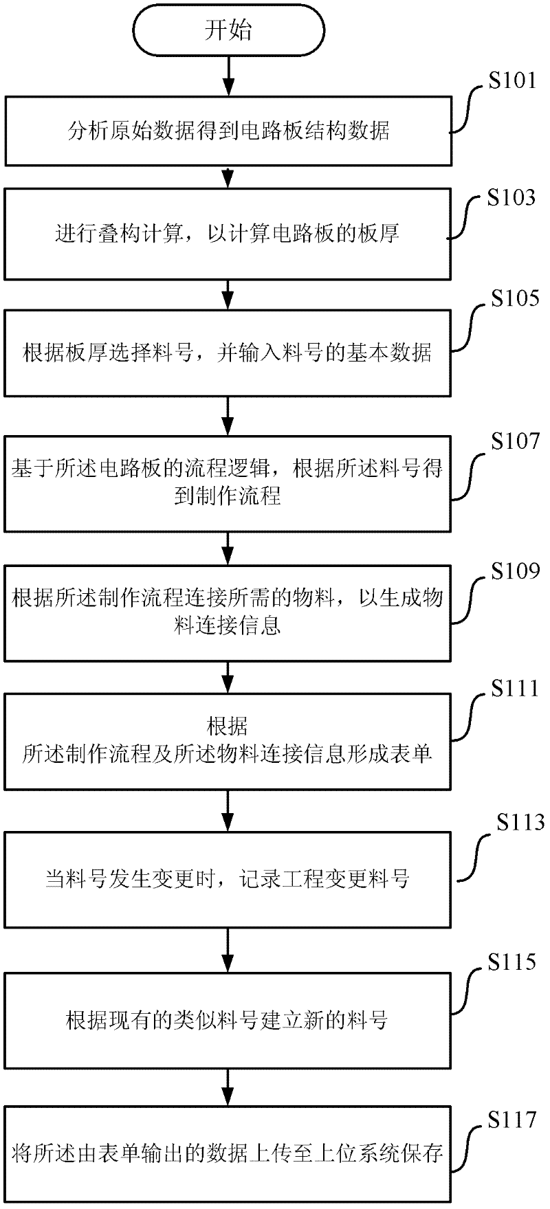
[0033] now refer to figure 2 An embodiment of the design method according to the present invention is described.

[0034] Such as figure 2 As shown, in step S101, the original circuit diagram of the circuit board is analyzed to obtain the structural data of the circuit board. Generally, the original circuit diagram comes from the customer's Gerber data.

[0035] In a preferred embodiment, it includes reading the origi...


PUM


Abstract

The invention discloses a design method of a flexible printed circuit board, comprising the following steps of: (1) analyzing the original circuit diagram of the circuit board to obtain structural data of the circuit board; (2) carrying out superposition calculation based on the structural data and the requirement of a consumer to calculate the thickness of the circuit board so as to obtain a superposition way for making a part number; (3) selecting the part number for the circuit board according to the calculated thickness of the circuit board, inputting basic data of the part number, and inspecting whether the thickness of the circuit board, corresponding to the part number, is matched with the calculated thickness of the circuit board to determine the selected part number; (4) obtaining a making process flow based on the process flow logic of the circuit board and according to the part number; (5) connecting required material according to the making process flow to generate material connection information; and (6) forming a form according to the making process flow and the material connection information.

Description

technical field [0001] The invention relates to a semiconductor design flow, in particular to a design method of a flexible printed circuit board (FPC). Background technique [0002] In the prior art, the design of a general flexible printed circuit needs to be completed in multiple systems. [0003] figure 1 with figure 2 An exemplary design approach is shown. Such as figure 1 As shown, first, the process and materials must be manually edited in System A. After that, the material number parameter must be entered in the B system. If there is an engineering change, the engineering change number (ECN) must also be entered in the C system. [0004] In this way, the entire design process becomes very complicated. Data analysis is performed in one system first, then in the editing process, followed by connecting materials, and finally saving the data. Thereafter, it is necessary to switch to the next system, and then carry out parameter input for the process in the previ...

Claims


Application Information

Patent Timeline
Patent Type & Authority Applications(China)
IPC IPC(8): G06F17/50
Inventor 陈红嫣周群江风
Owner 欣兴同泰科技(昆山)有限公司
Why Eureka
Try Eureka