Plugging device and circuit substrate plugging method

A circuit substrate, circuit substrate fixing technology, applied in the direction of electrical connection formation of printed components, etc., can solve problems such as incomplete filling, screen loss, poor reliability of plug hole processing, etc., to achieve the effect of improving efficiency and ensuring reliability

Inactive Publication Date: 2012-02-08
AVARY HLDG (SHENZHEN) CO LTD +1
View PDF4 Cites 12 Cited by
  • Summary
  • Abstract
  • Description
  • Claims
  • Application Information

AI Technical Summary

Problems solved by technology

Because there is air in the through hole of the circuit substrate, the gas in the through hole cannot be completely removed during the printing process, resulting in bubbles in the plugging material in the through hole or incomplete filling of th

Method used


Image

  • Plugging device and circuit substrate plugging method
  • Plugging device and circuit substrate plugging method
  • Plugging device and circuit substrate plugging method

Examples


Embodiment Construction

[0050] The plugging device provided by the technical solution will be further described below in conjunction with multiple drawings and embodiments.

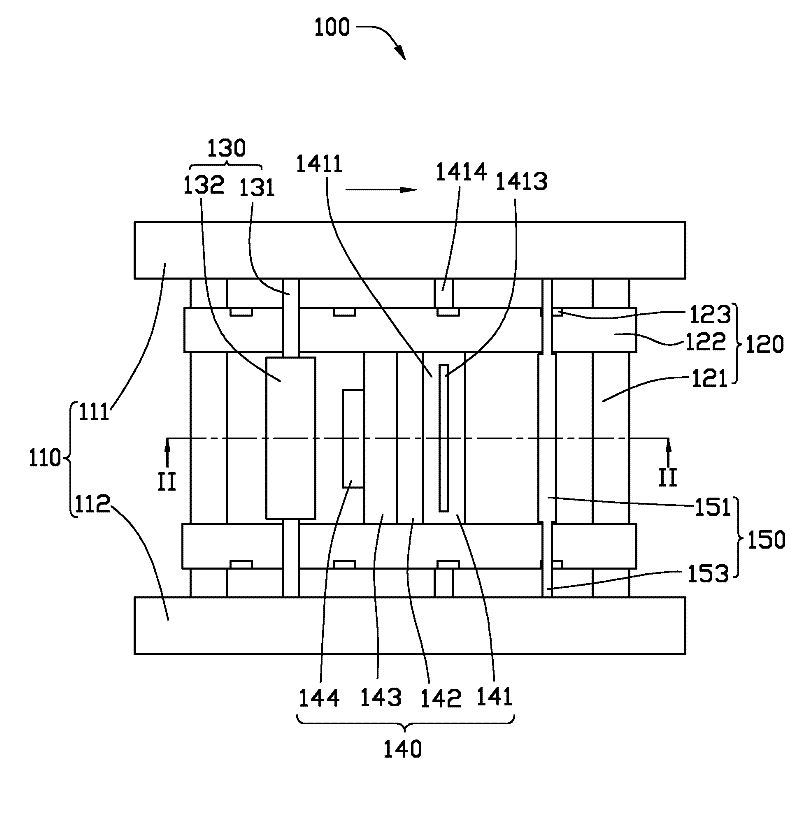
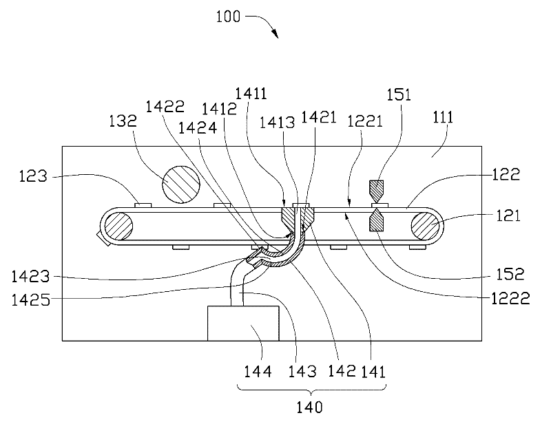
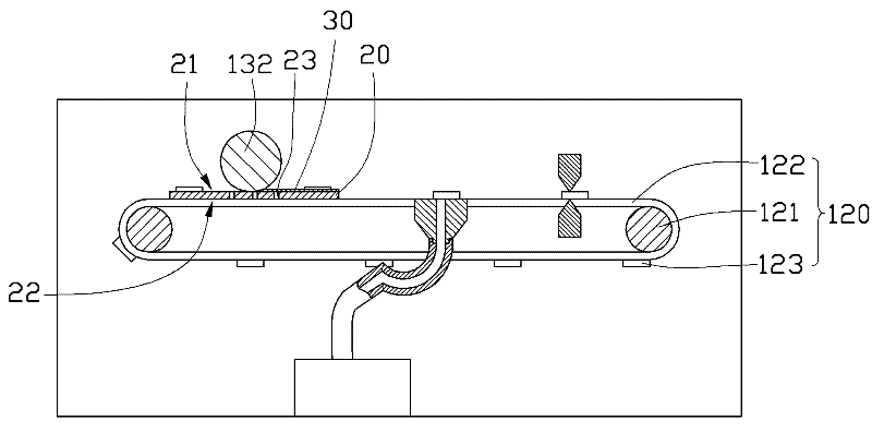
[0051] Please also refer to figure 1 and figure 2 , the embodiment of the technical solution provides a plugging device 100 for plugging via holes in a circuit substrate. The plugging device 100 includes a machine 110 , a conveying device 120 , a coating device 130 , an ink suction device 140 and an ink removing device 150 .

[0052] The machine platform 110 is used for carrying the conveying device 120 , the coating device 130 , the suction ink guiding device 140 and the ink removing device 150 . In this embodiment, the machine table 110 includes a first carrier 111 and a second carrier 112 . Both the first carrier 111 and the second carrier 112 are substantially rectangular plate-shaped and arranged parallel to each other. Both the first carrier 111 and the second carrier 112 are arranged along the conveying direction of ...


PUM


Abstract

The invention provides a plugging device which is used for plugging a through hole in a circuit substrate. The circuit substrate has an upper surface and a lower surface which are opposite, and the through hole penetrates through the upper surface and the lower surface. The plugging device comprises a conveying device, a coating device, a gas sucking and ink guiding device and an ink removing device, wherein the conveying device is used for conveying the circuit substrate to enable the circuit substrate to sequentially pass through the coating device, the gas sucking and ink guiding device and the ink removing device; the coating device is positioned above the conveying device and is used for coating a plugging material on the upper surface of the circuit substrate conveyed by the conveying device; the gas sucking and ink guiding device is positioned below the circuit substrate conveyed by the conveying device, is in contact with the lower surface of the circuit substrate, and is used for enabling the plugging material on the upper surface of the circuit substrate to enter the through hole by gas suction; and the ink removing device is positioned near the circuit substrate conveyed by the conveying device, and is used for removing the plugging material on the upper surface of the circuit substrate after plugging. The invention also relates to a method for plugging the circuit substrate by adopting the plugging device.

Description

technical field [0001] The invention relates to the technical field of circuit board production, in particular to a plugging device used in the circuit board production process and a method for plugging holes in a circuit substrate using the same. Background technique [0002] With the advancement of science and technology, printed circuit boards have been widely used in the electronic field. For the application of the circuit board, please refer to the literature Takahashi, A.Ooki, N.Nagai, A.Akahoshi, H.Mukoh, A.Wajima, M.Res.Lab, High density multilayer printed circuit board for HITAC M-880, IEEE Trans. on Components, Packaging, and Manufacturing Technology, 1992, 14(4): 418-425. [0003] In the actual production process of the circuit board, a via hole needs to be formed between the two conductive layers of the circuit board, so that the subsequently formed two-layer conductive lines are electrically connected to each other. The via hole is usually formed by the follow...

Claims


Application Information

Patent Timeline
IPC IPC(8): H05K3/40
Inventor 林钊文
Owner AVARY HLDG (SHENZHEN) CO LTD
Why Eureka
Try Eureka