Method for turning complicated optical curved surface by utilizing equal chip loads

A chip load and curved surface technology, applied in the field of complex optical precision manufacturing, can solve problems such as error convergence, reduced cutting efficiency, and weak rigidity

Active Publication Date: 2013-03-06
HUAWEI TEHCHNOLOGIES CO LTD
View PDF2 Cites 0 Cited by
  • Summary
  • Abstract
  • Description
  • Claims
  • Application Information

AI Technical Summary

Problems solved by technology

[0004] However, using the constant radial feed turning method to create complex optical surfaces inevitably has a very large chip load disturbance and depends on the coordinates of the tool contact or tool position, which will inevitably lead to significant disturbance of the cutting force
In complex optical surface turning systems, the FTS device or S 3 The motion axis is a link with relatively weak rigidity, so it will seriously affect the obtained surface shape accuracy under the action of disturbing cutting force
In existing utilizing FTS or S 3 In turning, in order to eliminate the surface error caused by cutting force disturbance, it is often necessary to perform multiple repeated error corrections, which reduces the cutting efficiency, and multiple repeated error corrections may not necessarily lead to error convergence.

Method used


Image

  • Method for turning complicated optical curved surface by utilizing equal chip loads
  • Method for turning complicated optical curved surface by utilizing equal chip loads
  • Method for turning complicated optical curved surface by utilizing equal chip loads

Examples


Embodiment Construction

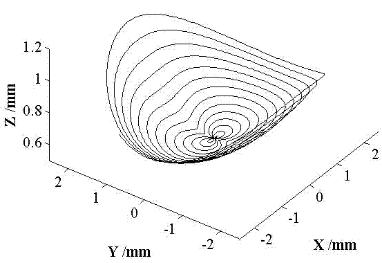
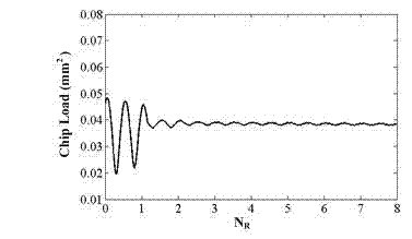
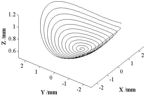
[0049] (1) According to the target optical surface, respectively create the surface to be processed in the first pass and the desired optical surface, and generate the tool path of the first pass with the goal of "equal chip load";

[0050] (2) Carry out on-machine or off-machine actual measurement of the machined surface created by the first tool pass, respectively create the surface to be machined and the expected optical surface created by the second tool pass, with the goal of "equal chip load" Generate the tool location path for the second tool pass;

[0051] (3) The "equal chip load" tool path generated for the two tool passes uses the two reciprocating motions of the two-degree-of-freedom fast tool servo and the spindle of the high-precision CNC lathe, x axis and z The non-reciprocating motion of the axis is realized.

[0052] A method for turning complex optical curved surfaces with equal chip loads, comprising the following steps:

[0053] (1) Create the initial su...


PUM


Abstract

The invention relates to a method for turning a complicated optical curved surface by utilizing equal chip loads, belonging to the field of complicated optical precision manufacturing. The method provided by the invention comprises the following steps: according to a target optical curved surface, respectively establishing a surface to be machined of the first pass and an expected optical curved surface and generating a cutter spacing path of the first pass by taking the equal chip loads as the target; carrying out on-machine or off-machine actual measurement on the machined surface obtained by the first pass, respectively establishing a surface to be machined for the second pass and an expected optical curbed surface, and generating the cutter spacing path of the second pass by taking the equal chip loads as the target; and synchronously realizing the cutter spacing paths generated in the two passes by utilizing the reciprocating motion of a two-freedom fast tool servos and the non-reciprocating motion of the principal axis, x axis and z axis of a high-accuracy numerically controlled lathe. The method has the advantages that the surface shape error caused by cutting force disturbance can be eliminated through the successive two passes; and the complicated optical curved surface can be cut and established without an expensive multi-axis super-accuracy lathe.

Description

technical field [0001] The invention belongs to the field of complex optical precision manufacturing, in particular to a method for turning complex optical curved surfaces with equal chip load. Background technique [0002] Complex optical surfaces include two connotations: one refers to rotationally symmetric aspheric optical surfaces with non-monotonic axis-section curves; the other refers to optical surfaces without rotational symmetry. [0003] Optical components with complex curved surfaces have a wide range of application requirements in many important industrial fields such as aerospace, national defense, and scientific instruments, as well as civilian optoelectronic products. How to create optical surfaces with complex geometric features and high-quality requirements efficiently and at low cost It has become one of the keys to promote the development of these fields. So far, the creation methods of complex optical surfaces mainly involve: replication forming, grindi...

Claims


Application Information

Patent Timeline
Patent Type & Authority Patents(China)
IPC IPC(8): B23B1/00
Inventor 周晓勤罗丹林洁琼
Owner HUAWEI TEHCHNOLOGIES CO LTD
Why Eureka
Try Eureka