Schottky diode with high reverse-blocking performance and manufacturing method thereof

A Schottky diode, high reverse technology, used in semiconductor/solid-state device manufacturing, electrical components, circuits, etc., can solve the problem of reverse leakage current saturation, reverse blocking characteristics, and reverse blocking characteristics. Softening and other problems, to achieve the effect of low forward voltage, reduced reverse leakage current, and increased reverse blocking voltage

Inactive Publication Date: 2012-02-15
丹东安顺微电子有限公司
View PDF8 Cites 23 Cited by
  • Summary
  • Abstract
  • Description
  • Claims
  • Application Information

AI Technical Summary

Problems solved by technology

The semiconductor region of the Schottky diode needs to adopt a lightly doped and thick drift region structure to withstand reverse blocking. To obtain high blocking capability, the current processing technology can only increase the thickness and resistivity of the drift region, but this will make the drift region The equivalent series resistance increases rapidly with the increase of the reverse breakdown voltage in a square relationship, and the forward voltage drop also increases significantly, and the reverse blocking characteristics become soft, resulting in a large reverse leakage current, so it will be strictly limited Application of Schottky Diodes in High Blocking Voltage Environment
Since the increase of the reverse blocking voltage is also affected by the lowering of the Schottky barrier, the reverse blocking characteristics are deteriorated, the blocking voltage is low, and the reverse leakage current is not saturated, so the reverse of the general Schottky diode The blocking voltage can only be within 100V, and it cannot be applied to high-voltage circuits with a reverse blocking voltage of 200V.

Method used


Image

  • Schottky diode with high reverse-blocking performance and manufacturing method thereof
  • Schottky diode with high reverse-blocking performance and manufacturing method thereof
  • Schottky diode with high reverse-blocking performance and manufacturing method thereof

Examples


Embodiment Construction

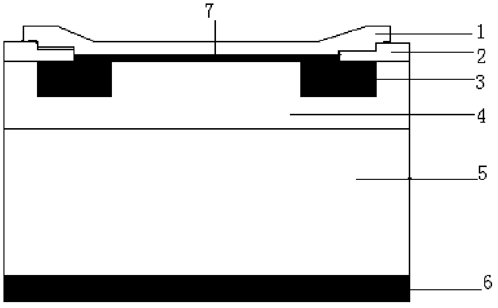
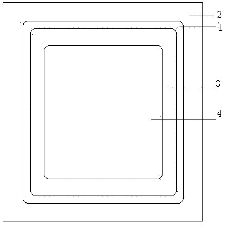
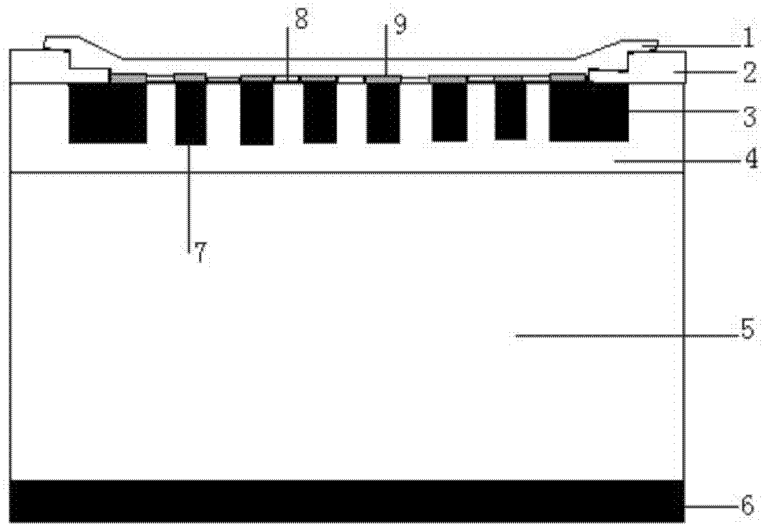
[0012] The patent application of the present invention discloses a Schottky diode with high reverse blocking performance, and its die structure is as follows: image 3 and Figure 4 As shown, its composition includes a heavily doped silicon substrate 5, epitaxially growing a lightly doped epitaxial layer 4 doped with P or AS as a drift region on the heavily doped silicon substrate 5, and implanting ions into the lightly doped epitaxial layer The P-type structure area made, and the upper and lower lead-out electric boards 1,6. The P-type structure region is composed of a P-type ring 3 and a P-type lattice 7 uniformly distributed in the epitaxial layer of the P-type ring 3, and the distance between the nearest adjacent P-type points of the P-type lattice is 5 In the range of -10um, the surface of the epitaxial layer in the P-type ring 3 has a metal layer 8 in Schottky barrier contact, the surface of the P-type structure region has an ohmic metal contact, and the outer edge of t...


PUM


Abstract

The invention provides a schottky diode with high reverse-blocking performance and a manufacturing method thereof. The schottky diode core is structurally characterized in that: a lightly doped epitaxial layer of a drift region is provided with a P-type structure region which is composed of a P-type ring and P-type dot matrixes uniformly spaced on the epitaxial layer in the P-type ring; the surface of the epitaxial layer in the P-type ring is provided with a schottky potential barrier contact metal layer; and the surface of the P-type structure region is in Ohm metal contact. When the schottky diode is in reverse application, a PN junction depletion region gradually spreads to a channel region along with the increase of the reverse voltage until the depletion region is communicated, and extends towards the substrate along with further increase of the reverse voltage to form an effective potential barrier in the channel region and effectively shield the schottky potential barrier region, thereby improving the reverse blocking ability that the reverse blocking voltage can reach 200 V or above; and moreover, the schottky diode also has good technical indexes such as reverse recovery time, reverse leakage current and the like, realizes low working loss of switches and prevents noise.

Description

technical field [0001] The invention relates to a Schottky diode and a manufacturing method thereof, in particular to a Schottky diode with improved reverse blocking characteristics and a manufacturing method thereof. Background technique [0002] Schottky diode is a high-current, ultra-high-speed, low-power rectification semiconductor device. It is an ideal device for high-frequency, low-voltage, high-current rectification, freewheeling and switch protection. Power electronic devices are gradually developing into high-frequency technology. It also promotes the technical development of Schottky diode technology in reducing power consumption and improving efficiency. It is a semiconductor device made of the metal-semiconductor junction principle that uses the surface barrier of the metal-semiconductor contact surface to produce rectification characteristics. The difference from the PN junction semiconductor device is that the Schottky diode is relatively conductive with minor...

Claims


Application Information

Patent Timeline
Patent Type & Authority Applications(China)
IPC IPC(8): H01L29/06H01L29/872H01L21/329
Inventor 杨建勋张子刚
Owner 丹东安顺微电子有限公司
Why Eureka
Try Eureka