Simulation method, device and system for high speed signal channel via holes

A high-speed signal and simulation method technology, applied in the field of electronic information, can solve problems such as low simulation efficiency, and achieve the effect of improving simulation accuracy, improving simulation efficiency, and saving simulation design time.

Inactive Publication Date: 2012-02-29
ZTE CORP
View PDF5 Cites 18 Cited by
  • Summary
  • Abstract
  • Description
  • Claims
  • Application Information

AI Technical Summary

Problems solved by technology

[0012] The purpose of the present invention is to provide a simulation method, device and system for hi

Method used


Image

  • Simulation method, device and system for high speed signal channel via holes
  • Simulation method, device and system for high speed signal channel via holes
  • Simulation method, device and system for high speed signal channel via holes

Examples


Embodiment approach

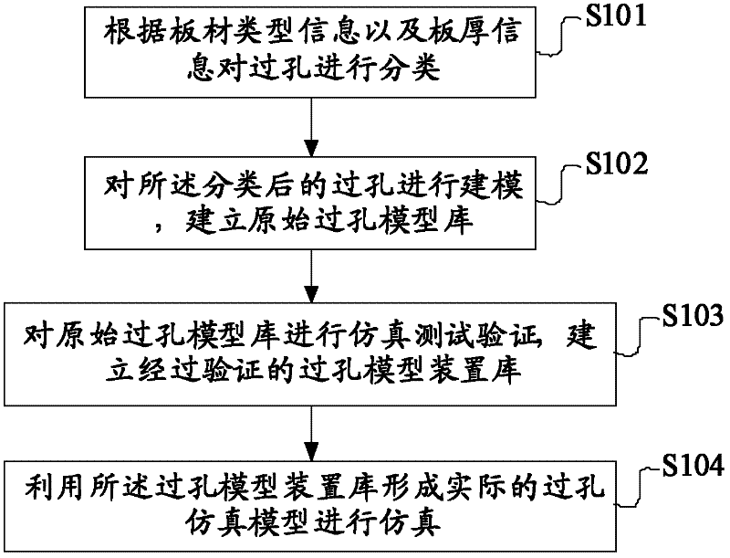
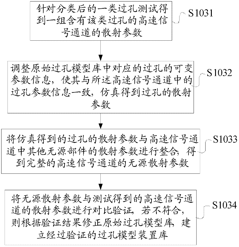
[0067] Under the preferred embodiment, as figure 2 As shown, in the step S103, the simulation test verification is performed on the original via model library, and the method for establishing a verified via model device library includes;

[0068] S1031. Obtain a set of scattering parameters of a high-speed signal channel containing this type of via according to the sorted via hole test;

[0069] S1032. Adjust the variable parameter information of the corresponding via in the original via model library to make it consistent with the via parameter information in the high-speed signal channel, and obtain the scattering parameters of the via through simulation;

[0070] S1033. Integrate the scattering parameters of the via holes obtained through simulation with the scattering parameters of other passive components in the high-speed signal channel to obtain complete passive scattering parameters of the high-speed signal channel;

[0071] S1034. Compare and verify the passive scat...


PUM


Abstract

The invention discloses a simulation method, a simulation device and a simulation system for high speed signal channel via holes. The method comprises the following steps of: classifying the via holes according to type information and plate thickness information of a plate material; modeling the classified via holes and constructing an original via hole model library; performing simulation test verification on the original via hole model library and constructing a verified via hole model device library; and forming an actual via hole simulation model for simulation by using the via hole model device library. Compared with the prior art, the simulation method, the simulation device and the simulation system for the high speed signal channel via holes have the advantages that: the high speed signal channel via hole simulation efficiency is improved, the time of high speed signal passive channel simulation design is shortened, and the simulation accuracy is improved.

Description

technical field [0001] The present invention relates to the field of electronic information technology, in particular to a simulation method, device and system for via holes of high-speed signal channels. Background technique [0002] Today's telecommunication systems, data communication systems, and computer systems all rely on the transmission of high-speed serial data. Even the system rate reaches 6.25Gbps, and the backplane standard of 10Gbps Ethernet has also been developed as a part of the 802.3ap standard. In order to complete the design of the chip-to-chip high-speed signal path system on the entire backplane, complex simulation, design, and test verification processes are required. [0003] In a typical high-speed interconnection system, the signal is driven by the chip on the single board, passes through the single board, the connector backplane, the connector and another single board, and reaches the receiving end chip. The passive path in this system is the mai...

Claims


Application Information

Patent Timeline
IPC IPC(8): G06F17/50
Inventor 贾威孙安兵
Owner ZTE CORP
Why Eureka
Try Eureka