Thin film photoelectric conversion module
A technology of photoelectric conversion module and photoelectric conversion layer, applied in photovoltaic power generation, energy conversion devices, circuits, etc., can solve problems such as hot spot phenomenon, current inability to flow, high impedance, etc.
- Summary
- Abstract
- Description
- Claims
- Application Information
AI Technical Summary
Problems solved by technology
Method used
Image

Examples
Embodiment Construction
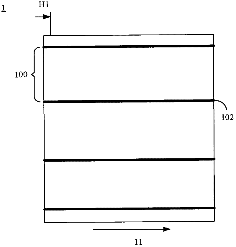
[0043] Please also refer to Figure 1A and Figure 1B . Figure 1A It is a top view of the thin film photoelectric conversion module 1 in an embodiment of the present invention, and Figure 1B for Figure 1A The side cross-sectional view of the thin film photoelectric conversion module 1 along the H1 direction.
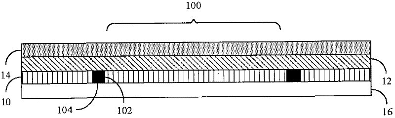
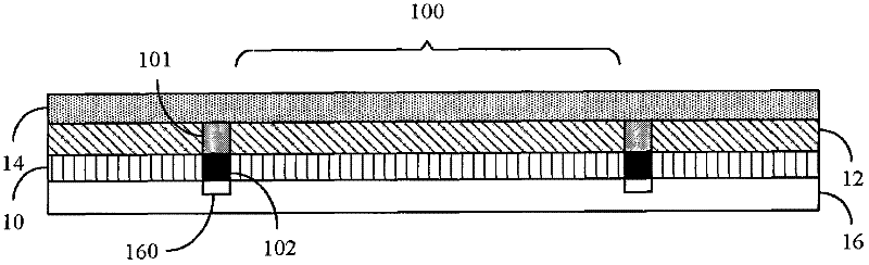
[0044] The thin film photoelectric conversion module 1 sequentially includes a substrate 16 , a first electrode layer 10 , a photoelectric conversion layer 12 and a second electrode layer 14 . The first electrode layer 10 includes a plurality of first electrode rows 100 and an electrical resistive material 102 . In one embodiment, the first electrode layer 10 is a front electrode. The first electrode arrays 100 are substantially parallel to each other and extend along the direction of current flow, that is, along Figure 1A Extend in the horizontal direction 11. The direction of current flow is the direction in which current flows in the thin film photoelectric con...
PUM
 Abstract
Description
Claims
Application Information