Liquid crystal display element
一种液晶显示元件、液晶的技术,应用在非线性光学、仪器、光学等方向,能够解决透射率偏差、对比度偏差、液晶倒下方向不一致等问题,达到提高显示质量、减小取向混乱、取向均一化的效果
- Summary
- Abstract
- Description
- Claims
- Application Information
AI Technical Summary
Problems solved by technology
Method used
Image
Examples
Embodiment approach 1
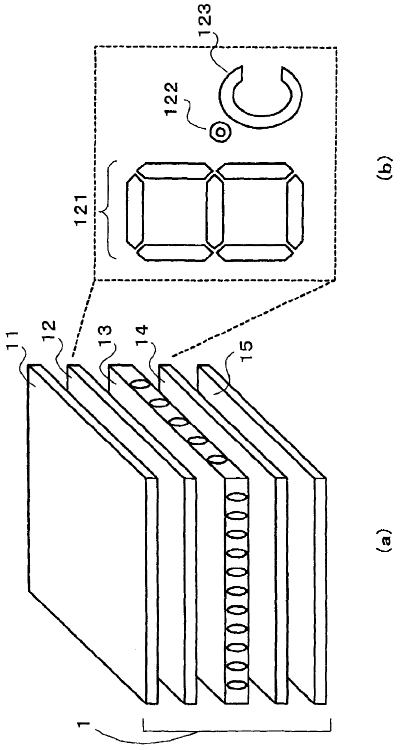
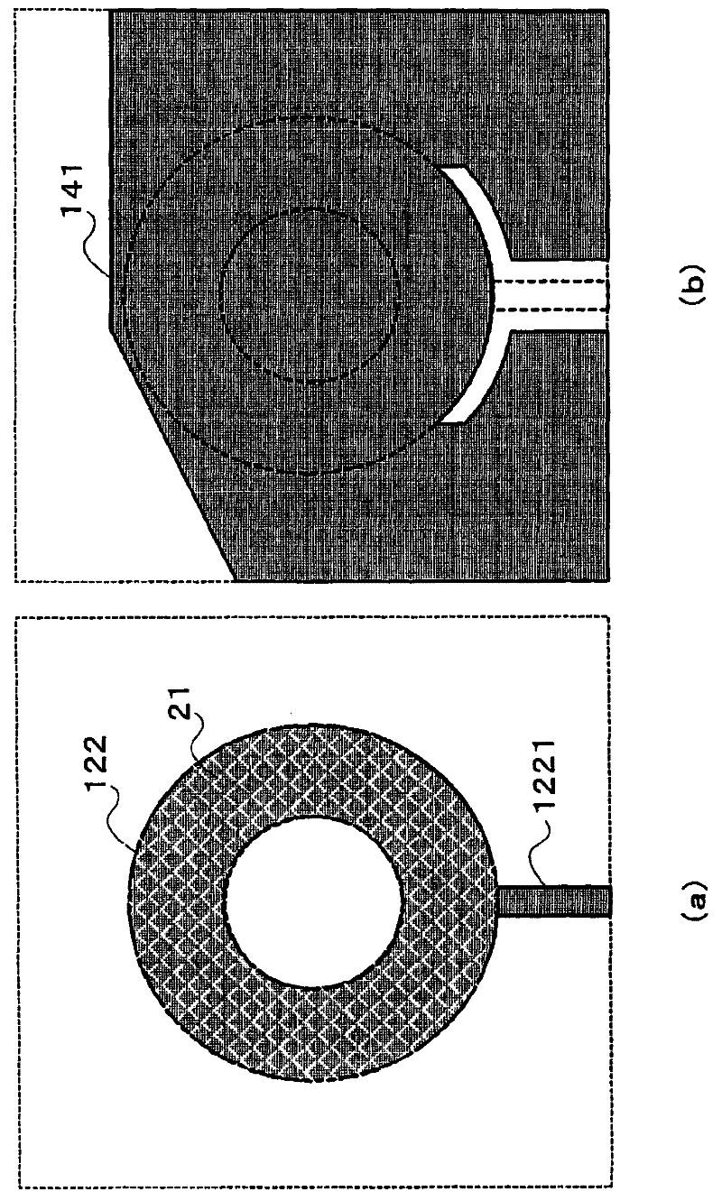
[0055] Hereinafter, embodiments of the present invention will be described with reference to the drawings. figure 1 (a) is an exploded perspective view showing a structural example of the VA-type liquid crystal display element 1 according to Embodiment 1 of the present invention. The liquid crystal display device 1 is formed between two substrates (not shown) such as glass, and has a structure in which a front polarizing plate 11, a segment electrode portion 12, and a liquid crystal layer are stacked as viewed from the visible side (front side). 13. A common electrode part 14 and a rear polarizing plate 15 . Hereinafter, the front polarizing plate 11 is referred to as an F polarizing plate 11 . The rear polarizing plate 15 is referred to as an R polarizing plate 15 . When no voltage is applied to the liquid crystal display element 1 , the liquid crystals in the liquid crystal layer 13 are aligned vertically. In addition, the F polarizer 11 and the R polarizer 15 are arrang...
Embodiment approach 2
[0075] Next, Embodiment 2 of the present invention will be described. In this embodiment mode, the present invention is applied to a dot-matrix VA-type liquid crystal display device. Figure 8 (a) is an exploded perspective view showing a structural example of a VA-type liquid crystal display element 1 according to Embodiment 2, and is basically the same as figure 1 The structure shown in (a) is the same. That is, the liquid crystal display element 1 is formed between two substrates such as glass, and has a structure in which an F polarizing plate 11, a segment electrode portion 12, a liquid crystal layer 13, a common electrode portion 14, and R polarizer 15. exist Figure 8 Also in (a), the description of the substrate is omitted.
[0076] Figure 8 (b) is a plan view showing an example of the segment electrode portion 12 and the common electrode portion 14 of the present embodiment. exist Figure 8 In (a), the plate-shaped segment electrode portion 12 is shown, but m...
Embodiment 1
[0088] Specific examples will be described below. In addition, this Example (Example 1) and Examples 2 to 4 described later are examples corresponding to Embodiment 1, and Examples 5 to 7 are examples corresponding to Embodiment 2.
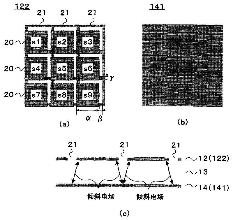
[0089] Figure 11 (a) is an enlarged plan view of a part of the segment electrode of the first embodiment. Such as Figure 11 As shown in (a), in this embodiment, the segment electrodes conforming to the shape of the display pattern are patterned on the glass substrate on the F side (viewable side), so that by regularly forming the width of the segment electrodes in the area of the segment electrodes It is an L-shaped groove of 10 μm, so that one side thereof includes a plurality of sub-pixel electrodes of 55×55 μm. Each sub-pixel electrode 20 has a shape in which connection portions for connecting to other sub-pixel electrodes are provided at three corners.
[0090] In addition, on the glass substrate on the R side (opposite to the visible ...
PUM
| Property | Measurement | Unit |
|---|---|---|
| diameter | aaaaa | aaaaa |
| width | aaaaa | aaaaa |
| diameter | aaaaa | aaaaa |
Abstract
Description
Claims
Application Information


