
Local thick copper plating process of dense hole

A technology of local plating and dense holes, which is applied in the direction of assembling printed circuits of electrical components and secondary treatment of printed circuits, etc., can solve the problems of inability to meet the requirements of local thick copper plating, achieve good working conditions, prolong service life, and ensure stability running effect

Active Publication Date: 2012-04-25
DONGGUAN SHENGYI ELECTRONICS
View PDF4 Cites 13 Cited by
  • Summary
  • Abstract
  • Description
  • Claims
  • Application Information

AI Technical Summary

Problems solved by technology

However, the traditional PCB manufacturing process cannot meet the local thick copper plating requirements. Therefore, it is necessary to develop a processing method for this type of PCB.

Method used


Image

  • Local thick copper plating process of dense hole
  • Local thick copper plating process of dense hole
  • Local thick copper plating process of dense hole

Examples


Embodiment Construction

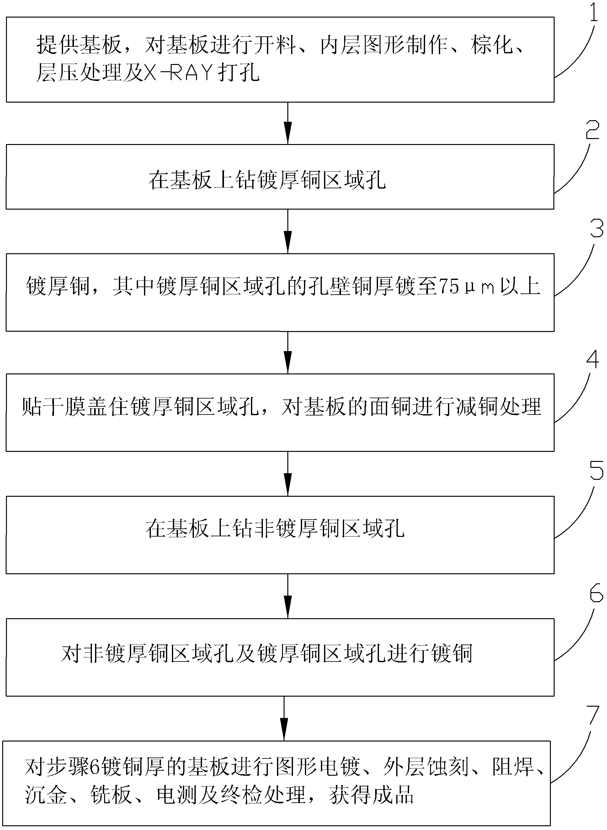
[0022] Such as figure 1 Shown, be the flow chart of dense hole local thick copper plating process of the present invention, this process comprises the steps:

[0023] Step 1. Provide the substrate, carry out material cutting, inner layer pattern making, browning, lamination treatment and X-ray (X-RAY) drilling (punching the first set of positioning targets) on the substrate; this step can be achieved through the existing technology accomplish.

[0024] Step 2. Drill holes in the thick copper plated area on the substrate.

[0025] Step 2.1: Baking board treatment, the baking board condition is 150-180°C for 5 hours (h).

[0026] Step 2.2. Perform deburring treatment on the holes in the thick copper plating area, such as removing the burrs of the drilled holes.

[0027] Step 3, thick copper plating, pulse parameters: 15-20ASF×(96min+96min), that is, electroplating with a current density of 15-20 amps / square foot (ASF) for 96 minutes (min), then turn the substrate around, and ...


PUM


Abstract

The invention provides a local thick copper plating process of a dense hole, which comprises the following steps of: 1, providing a substrate, carrying out cutting, inner-layer pattern manufacturing, browning, laminating and X-RAY punching on the substrate; 2, drilling a thick copper plating region hole on the substrate; 3, plating thick copper, wherein the copper is plated on the hole wall in the thick copper plating region hole until the thickness of the copper reaches 75mu m and above; 4, pasting a dry film to cover the thick copper plating region hole, carrying out copper reducing treatment on surface copper of the substrate; 5, drilling a non-thick-copper-plating region hole on the substrate; and 6, carrying out copper plating on the non-thick-copper-plating region hole and the thick-copper-plating region hole. By adopting a secondary drilling and secondary immersion copper process, a primary drilling and immersion copper process during the traditional PCB manufacture is changed, high heat generated when the element works is effectively conducted and radiated outside by using better heat conduction coefficient of the copper through designing local thick copper plating on a position of the PCB, thus demands of high-end electronic products in future to higher heat radiation performance required in a local region are met.

Description

technical field [0001] The invention relates to a thick copper plating process, in particular to a local thick copper plating process for dense holes. Background technique [0002] With the rapid development of high-integration component technology, the design of various components tends to be dense, and accordingly higher requirements are put forward for heat dissipation. The traditional hole wall copper thickness can no longer meet such design requirements; in order to meet the heat dissipation requirements, Correspondingly, the position of the local heat dissipation hole is required to be a local thick copper design (thick copper with dense holes is more conducive to heat dissipation), so as to meet the electrical performance and heat dissipation requirements of important components. However, the traditional PCB manufacturing process cannot meet the local thick copper plating requirements. Therefore, it is necessary to develop a processing method for this type of PCB. C...

Claims


Application Information

Patent Timeline
Patent Type & Authority Applications(China)
IPC IPC(8): H05K3/22H05K3/30
Inventor 辜义成曾志军曾红
Owner DONGGUAN SHENGYI ELECTRONICS
Features
  • Generate Ideas
  • Intellectual Property
  • Life Sciences
  • Materials
  • Tech Scout
  • Unparalleled Data Quality
  • Higher Quality Content
  • 60% Fewer Hallucinations
Learn More