Embedded memorizer and embedded memorizer system

An embedded memory and storage system technology, applied in memory systems, instruments, computing, etc., can solve problems such as poor storage capacity scalability, and achieve the effects of improving storage scalability, reducing storage costs, and improving controllability

Inactive Publication Date: 2012-05-02
忆正存储技术(武汉)有限公司
View PDF2 Cites 7 Cited by
  • Summary
  • Abstract
  • Description
  • Claims
  • Application Information

AI Technical Summary

Problems solved by technology

[0005] The main technical problem to be solved by the present invention is to provide an embedded memory and an embedded storage system, which can avoid the problem of poor storage capacity expansion caused by the solidification of the storage capacity on the embedded memory

Method used


Image

  • Embedded memorizer and embedded memorizer system
  • Embedded memorizer and embedded memorizer system
  • Embedded memorizer and embedded memorizer system

Examples


Embodiment 1

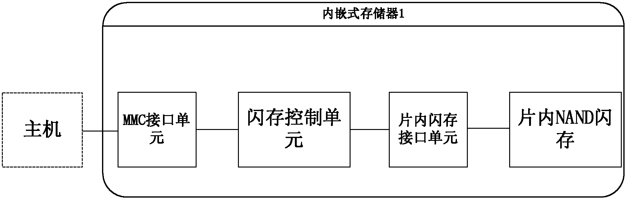
[0023] Please refer to figure 2 It is a structural schematic diagram of the embedded memory of the present invention. The embedded memory in this embodiment includes an on-chip NAND flash memory, a flash memory control unit, an MMC interface unit, an on-chip flash memory interface unit, and an off-chip flash memory interface unit. Please refer to image 3 , is a schematic structural diagram of Embodiment 1 of the embedded memory of the present invention. The off-chip flash memory interface of the embedded memory is not connected to any external storage device. It has been proved by experiments that no storage device is connected under the premise of adding an off-chip flash memory interface unit. The working status and working efficiency of the entire embedded memory are not affected. In addition, the NAND flash memory and the on-chip flash memory interface unit may not be provided on-chip. At this time, the NAND flash memory needs to be connected to the off-chip, and all...

Embodiment 2

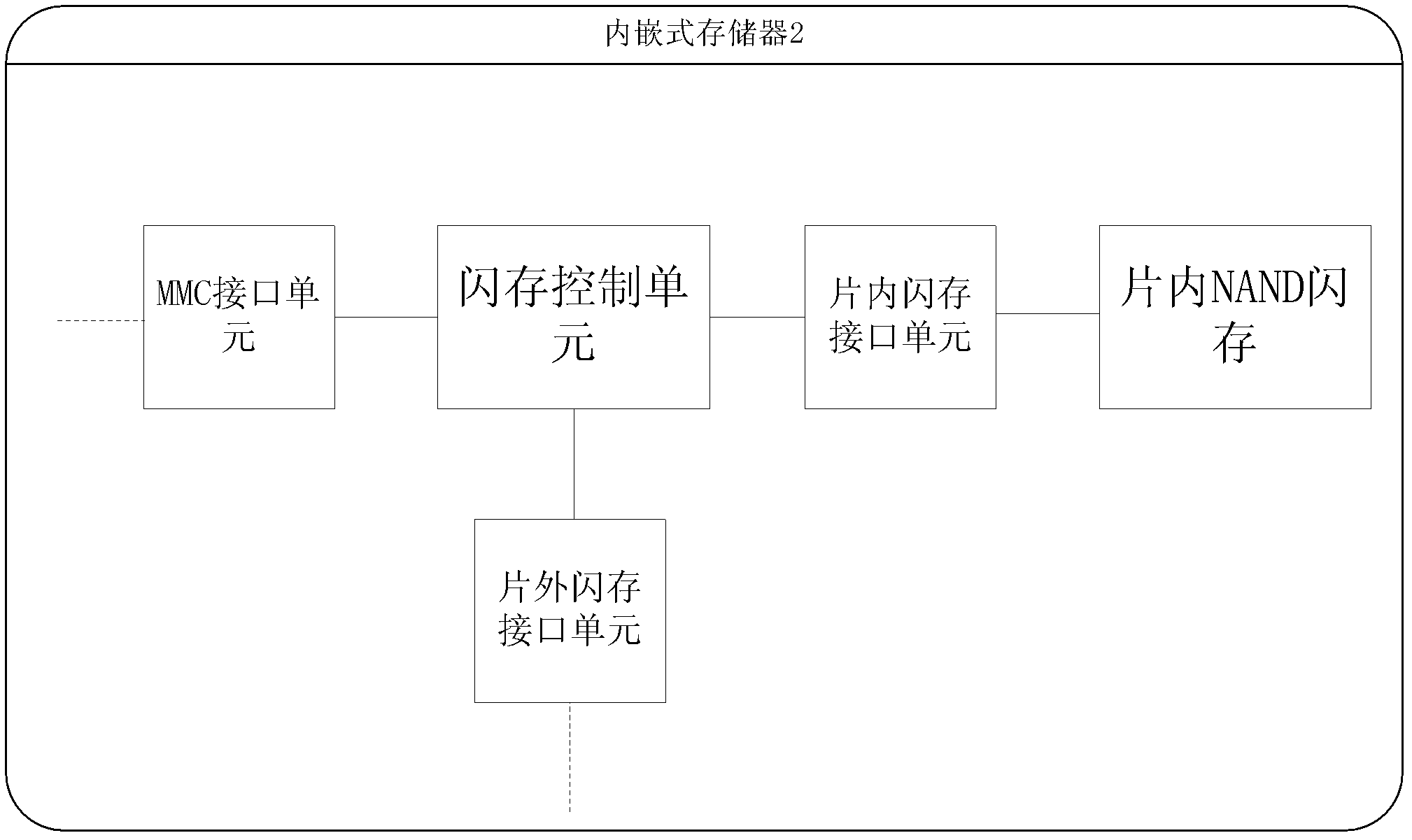
[0025] Please refer to Figure 4 , is a schematic structural diagram of Embodiment 2 of the embedded storage system of the present invention. The embedded storage system in this embodiment includes on-chip NAND flash memory, flash memory control unit, MMC interface unit, on-chip flash memory interface unit, off-chip flash memory interface unit, and the external end of the off-chip flash memory interface of the embedded memory Connect an off-chip NAND flash memory with a capacity larger than the on-chip NAND flash memory.

[0026] In this embodiment, since a large-capacity NAND flash memory is connected, the storage capacity is increased, thereby improving the storage scalability of the entire embedded storage system.

[0027] In this embodiment, the embedded storage system can also use multiple off-chip flash memory interfaces connected to the flash memory controller provided on the NC pins of the BGA package to access multiple off-chip NAND flash memories. The storage capac...

Embodiment 3

[0029] Please refer to Figure 5 , is a schematic structural diagram of Embodiment 3 of the embedded storage system of the present invention. The embedded storage system in this embodiment includes an on-chip NAND flash memory, a flash memory control unit, an MMC interface unit, an on-chip flash memory interface unit, an off-chip flash memory interface unit, and a large-capacity off-chip NAND flash memory. The off-chip NAND flash memory is connected to the off-chip flash memory interface. In this embodiment, the on-chip NAND flash memory is SLC NAND flash memory, and the off-chip NAND flash memory is TLC NAND flash memory.

[0030] In this embodiment, since the on-chip NAND flash memory and the flash memory controller are packaged in a BGA package, SLC NAND flash memory with a longer service life is selected in order to improve usage efficiency. The off-chip NAND flash memory uses TLC NAND flash memory with relatively low production cost. This not only improves the storage ...


PUM


Abstract

The invention discloses an embedded memorizer and an embedded memorizer system. The embedded memorizer comprises an on-chip NADN flash memory, a flash memory control unit, a multimedia card (MMC) interface unit, an on-chip flash memory interface unit and an off-chip flash memory interface. The embedded memorizer system comprises the embedded memorizer and one or a plurality of extended NAND flash memories. The extended NAND flash memories exchange data with the flash memory control unit through the off-chip flash memory interface. The embedded memorizer and the embedded memorizer system can avoid poor memorizer capacity expansion caused by the fact that the embedded memorizer has no redundant NAND flash memory interface to be connected with the off-chip NAND flash memory. Integral memorizer costs of products can be reduced through combination of the NAND flash memories of various types.

Description

technical field [0001] The invention relates to an embedded storage technology, in particular to an embedded storage and an embedded storage system with expandable storage capacity. Background technique [0002] The embedded memory is an extension of the external memory card MMC, which is widely used in the fields of mobile phone production and tablet PC (Tablet PC) applications. Please refer to figure 1 The structure of the embedded memory 1 includes: an MMC interface connected to the host, a flash memory control unit for managing flash memory, a piece of NAND flash memory, and an on-chip flash memory interface for realizing data interaction between the flash memory control unit and the NAND flash memory. An obvious advantage of the embedded memory is that the NAND flash memory and the flash memory controller are packaged in a small BGA package, and an external standard MMC interface is provided to the host. This not only solves the compatibility problem between NAND flas...

Claims


Application Information

Patent Timeline
Patent Type & Authority Applications(China)
IPC IPC(8): G06F13/16
CPCG06F13/16G06F13/4239G06F12/0246
Inventor 蔡孟宏李宽仁
Owner 忆正存储技术(武汉)有限公司
Why Eureka
Try Eureka