Organic light-emitting diode encapsulation structure and manufacturing method thereof

A technology for light-emitting diodes and packaging structures, which is applied in the manufacture of semiconductor/solid-state devices, electrical components, and electrical solid-state devices, etc., can solve the problems of absorbing water and oxygen, poor water and oxygen resistance of the packaging adhesive 14, and thick front sheet 11, etc. The effect of prolonging life and avoiding water and oxygen interference

Inactive Publication Date: 2012-05-09
CPTF VISUAL DISPLAY (FUZHOU) LTD +1
View PDF3 Cites 23 Cited by
  • Summary
  • Abstract
  • Description
  • Claims
  • Application Information

AI Technical Summary

Benefits of technology

The technical effect described by this patented technology relates to prevention of moisture or other gases ingress into an LED package during manufacturing process due to its design features. This helps maintain better performance over longer periods without losing any significant amount of power output.

Problems solved by technology

This patented technical problem addressed in this patents relating to improving the durability and lifespan of Organic Light Emission Diodes (OLEDS). Current methods for prevention from oxidizing or losing moieties due to exposures during shipping require expensive specialized equipment that increases costs compared to regular maintenance. Additionally, current techniques involve adding layers inside packages without adequate protection against external factors like humidity and airflow.

Method used


Image

  • Organic light-emitting diode encapsulation structure and manufacturing method thereof
  • Organic light-emitting diode encapsulation structure and manufacturing method thereof
  • Organic light-emitting diode encapsulation structure and manufacturing method thereof

Examples


Embodiment Construction

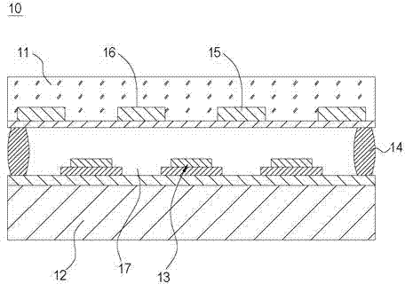
[0019] Please refer to Figure 2a to Figure 2c , which shows the manufacturing method of the OLED packaging structure 110 according to the first embodiment of the present invention.

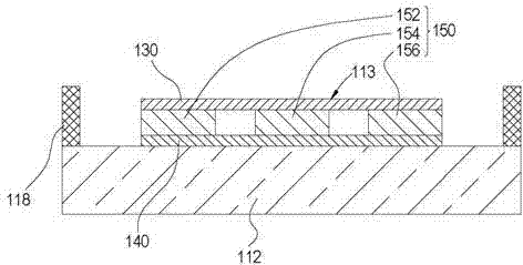
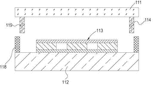
[0020] refer to Figure 2a As shown, a substrate 112 (such as a glass substrate) is provided, which defines a plurality of pixel areas, and each pixel area forms an organic light emitting element 113. The organic light emitting element 113 generally includes an anode layer 130 and a cathode layer 140, and a The organic semiconductor layer 150 , the organic semiconductor layer 150 includes a red light emitting layer 152 , a green light emitting layer 154 and a blue light emitting layer 156 and is disposed between the anode layer 130 and the cathode layer 140 . At least one of the above-mentioned anode layer 130 and cathode layer 140 is a transparent electrode, and the other can be a metal, a metal alloy, a transparent metal oxide, or a mixed layer of the above.

[0021] A retaining wall 118 is f...


PUM

PropertyMeasurementUnit
Widthaaaaaaaaaa

Abstract

A manufacturing method of an organic light-emitting diode encapsulation structure comprises the following steps of: forming an organic light-emitting component on a substrate; forming a retaining wall on the substrate, wherein the retaining wall is arranged on the periphery of the organic light-emitting component in a surrounding manner and is made of one of groups formed by calcium metal, magnesium metal, aluminum metal, carton, zinc metal, chromium metal, tin metal, lead metal and copper metal; forming a packaging plastic material on a cover plate; and bonding the cover plate with the substrate by using the packaging plastic material and then solidifying the packaging plastic material, wherein the packaging plastic material is arranged on the periphery of the organic light-emitting component in a surrounding manner, and the packaging plastic material and the retaining wall are positioned between the cover plate and the substrate to seal the organic light-emitting component.

Description


Claims


Application Information

Patent Timeline
Owner CPTF VISUAL DISPLAY (FUZHOU) LTD
Why Eureka
Try Eureka