Touch screen and manufacture method thereof

A production method and touch screen technology, applied in the direction of instruments, electrical digital data processing, data processing input/output process, etc., can solve the problems of thick resistive touch screen, hinder light transmission, low transmittance of resistive touch screen, etc., and achieve easy Multi-touch, achieve ultra-thin, enhance the effect of sensitivity

Inactive Publication Date: 2012-05-23
BOE TECH GRP CO LTD +1
View PDF2 Cites 0 Cited by
  • Summary
  • Abstract
  • Description
  • Claims
  • Application Information

AI Technical Summary

Problems solved by technology

Due to the existence of the cavity 013, the resistive touch screen is relatively thick and the cavity will seriously hinder the transmission of light, resulting in a low transmittance of the resistive touch screen
Similarly, there are similar deficiencies for capacitive touch screens

Method used


Image

  • Touch screen and manufacture method thereof
  • Touch screen and manufacture method thereof
  • Touch screen and manufacture method thereof

Examples


Embodiment 1

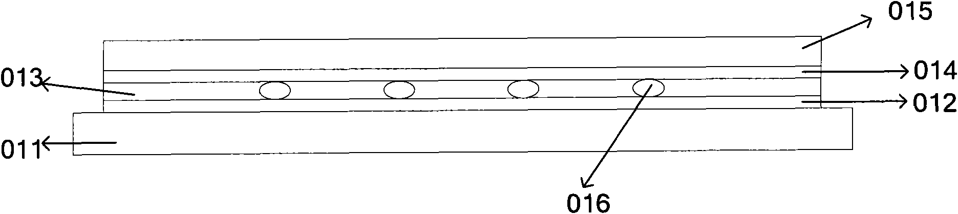
[0045] Such as figure 2 As shown, the touch screen provided in this embodiment includes a first substrate 01 and a second substrate 02 oppositely arranged and a touch screen controller, and a first circuit layer is formed between the first substrate 01 and the second substrate 02 and a second circuit layer 15, and an insulating layer 16 is formed between the first circuit layer and the second circuit layer 15;

[0046] The first circuit layer is used to sense the touch of external force, and the second circuit layer is used to transmit the signal of whether the touch point is touched by external force to the touch screen controller;

[0047]The first circuit layer includes at least one memory alloy node 12, and a circuit path 11 for supplying power to the at least one memory alloy node 12; in order to more clearly show the connection between the first circuit layer and the second circuit layer 15 The connection relationship, in the illustration, only the circuit connection o...

Embodiment 2

[0054] Such as Figure 5 As shown, the touch screen provided in this embodiment provides another implementation solution for the circuit design of the first circuit layer and the second circuit layer, and other designs are similar to the implementation solution of the first embodiment, and will not be repeated here.

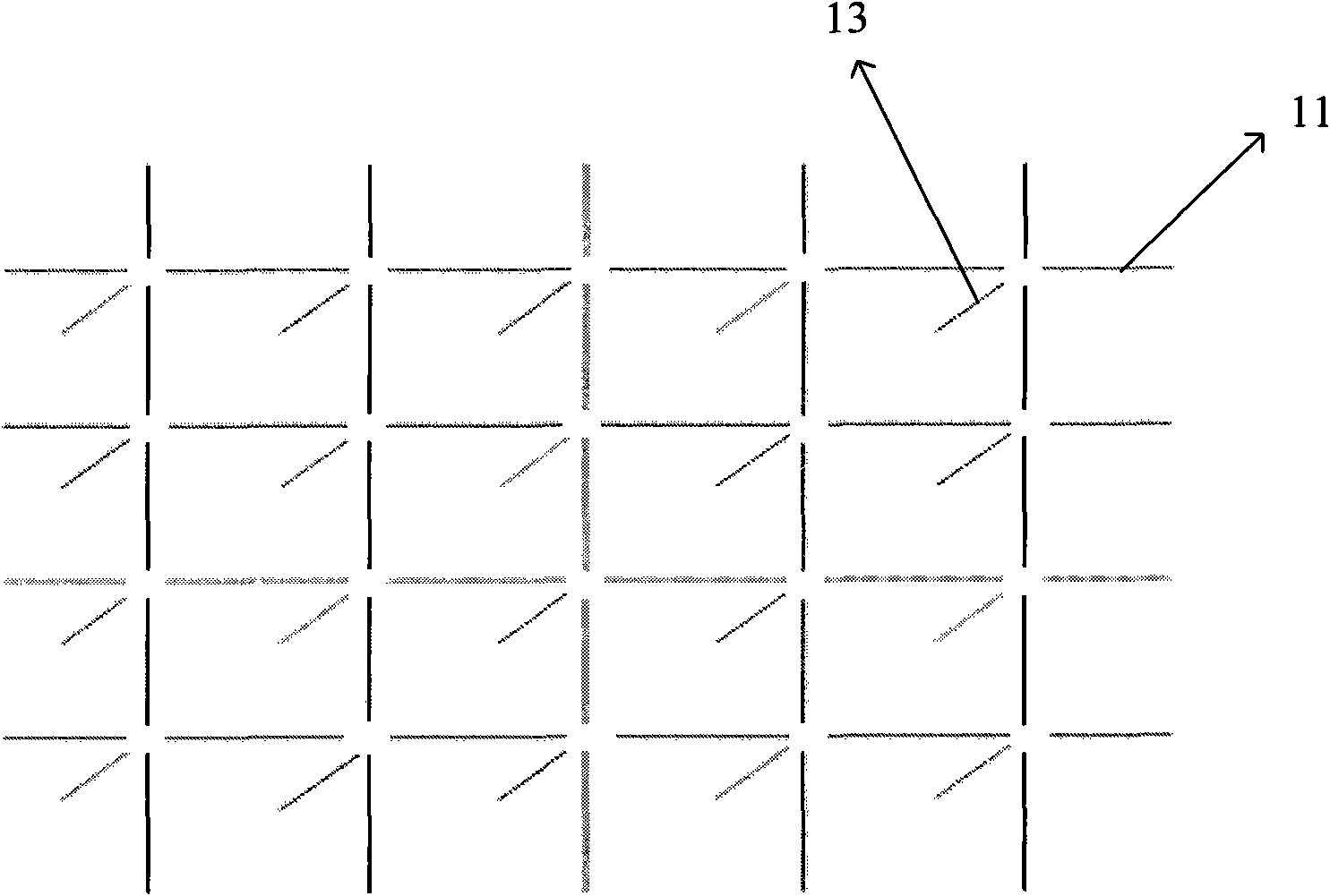
[0055] In this embodiment, the circuit path in the first circuit layer is Figure 6 The mesh structure shown, with no connections between line ends at each mesh node. A memory alloy node 12 is provided at each grid node, and the memory alloy node 12 is fixed on the first substrate 01 . An insulating layer 16 is provided between the first circuit layer and the second circuit layer 15, and a via hole 14 filled with ITO is provided on the insulating layer 16, and the via hole 14 is provided at the memory alloy node 12 directly below and in contact with the memory alloy node 12, and there is no electrical connection with all wire ends at the grid node.

[0056] Su...

Embodiment 3

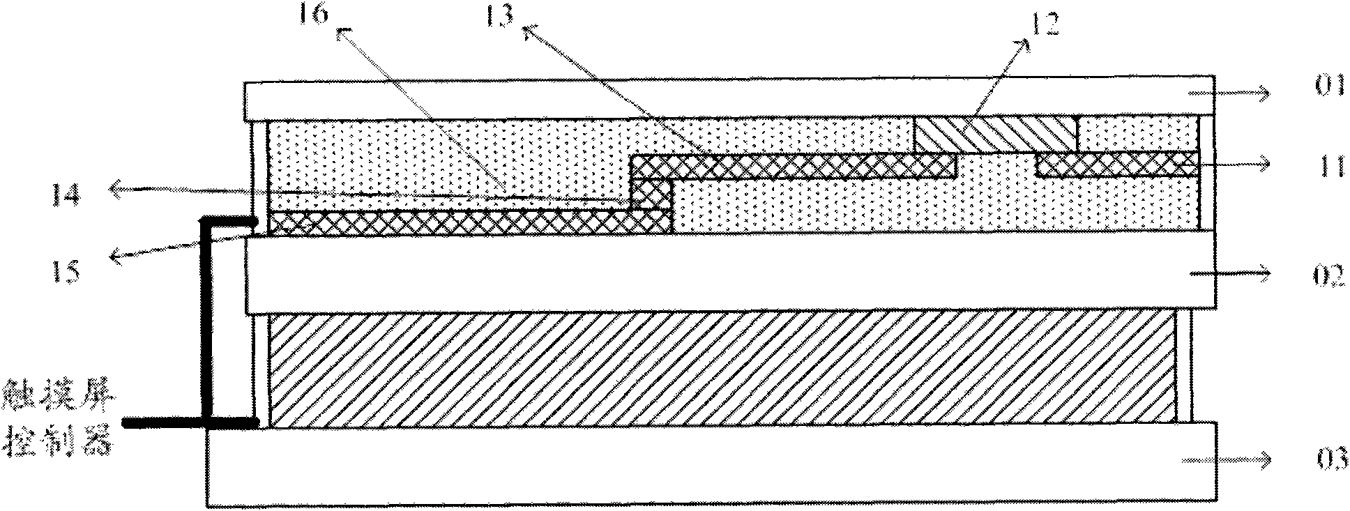
[0059] Such as Figure 7 As shown, the touch screen provided in this embodiment includes a first substrate 01 and a second substrate 02 oppositely arranged and a touch screen controller, and a first circuit layer is formed between the first substrate 01 and the second substrate 02 and a second circuit layer 15, and an insulating layer 16 is formed between the first circuit layer and the second circuit layer 15;

[0060] The first circuit layer includes at least one memory alloy node 12, and a circuit path 11 for powering the at least one memory alloy node 12; the second circuit layer 15 includes at least one wire connected to the touch screen controller , and each wire corresponds to a memory alloy node 12, so that the touch screen controller can detect the connection status between each memory alloy 12 and its corresponding wire.

[0061] Among them, in order to better sense the change of external force on the touch screen, soft plate glass is selected as the first substrate...


PUM


Abstract

The invention discloses a touch screen and a manufacture method of the touch screen, which relates to the field of liquid crystal display and has the advantages that the ultra-thin effect of the touch screen can be realized, and the light transmission rate is improved. The touch screen comprises a first base plate, a second base plate and a touch screen controller, wherein the first base plate and the second base plate are in opposite arrangement, a first circuit layer and a second circuit layer are formed between the first base plate and the second base plate, in addition, an insulating layer is formed between the first circuit layer and the second circuit layer, the first circuit layer comprises at least one memory alloy node and at least one closed circuit for supplying electricity to the memory alloy node, the second circuit layer comprises at least one conducting wire connected with the touch screen controller, and in addition, each conducting wire corresponds to one memory alloy node. In addition, the invention simultaneously discloses the manufacture method of the touch screen. The scheme provided by the invention is applicable to the touch screen.

Description

technical field [0001] The invention relates to a touch screen and a manufacturing method thereof. Background technique [0002] With people's demands for diversification, it is more and more popular to use a touch screen instead of a keyboard or a mouse to control a liquid crystal display device. Currently, the more commonly used touch screens are resistive touch screens and capacitive touch screens. [0003] Among them, the structure of the resistive touch screen is as follows: figure 1 As shown, it includes an upper substrate 015 , a lower substrate 011 , an upper conductive layer 014 , and a lower conductive layer 012 , and a spacer 016 is provided between the upper and lower conductive layers to form a cavity 013 . Due to the existence of the cavity 013, the resistive touch screen is relatively thick and the cavity will seriously hinder the transmission of light, resulting in a low transmittance of the resistive touch screen. Likewise, there are similar deficiencies ...

Claims


Application Information

Patent Timeline
Patent Type & Authority Applications(China)
IPC IPC(8): G06F3/041
Inventor 谢建云
Owner BOE TECH GRP CO LTD
Why Eureka
Try Eureka