


Quick Research
Generate reliable direction feasibility study reports for your R&D in just a few steps.

Technical Q&A
Discover and master advanced knowledge NOW. Basics, ideas, possibilities, all at once.

Find Solutions
As an expert in R&D theories, this can generate solutions to your technical problems instantly.

Evaluate Feasibility
Analyze your overall solution with one click, know your potential R&D risks in advance.

Monitor Landscape
Get weekly tech updates, stay abreast of the latest tech innovations and key insights.
Lens and semiconductor light-emitting element module using same
A light-emitting element module and semiconductor technology, which is applied in the direction of semiconductor devices, semiconductor devices, optical elements, etc. of light-emitting elements, and can solve problems such as the inability to reduce the width
- Summary
- Abstract
- Description
- Claims
- Application Information
AI Technical Summary
Problems solved by technology
Method used
Image

Examples
Embodiment Construction
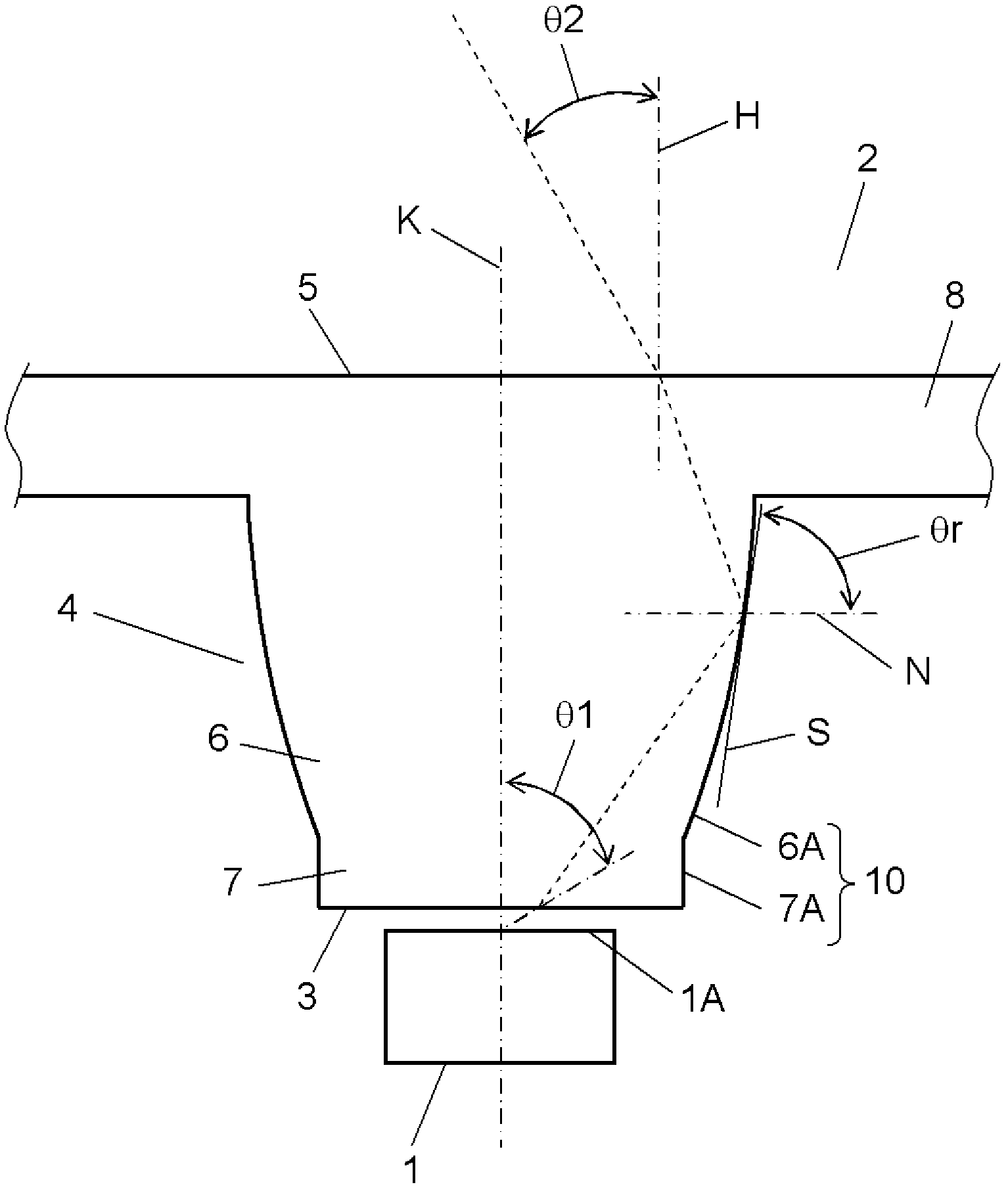
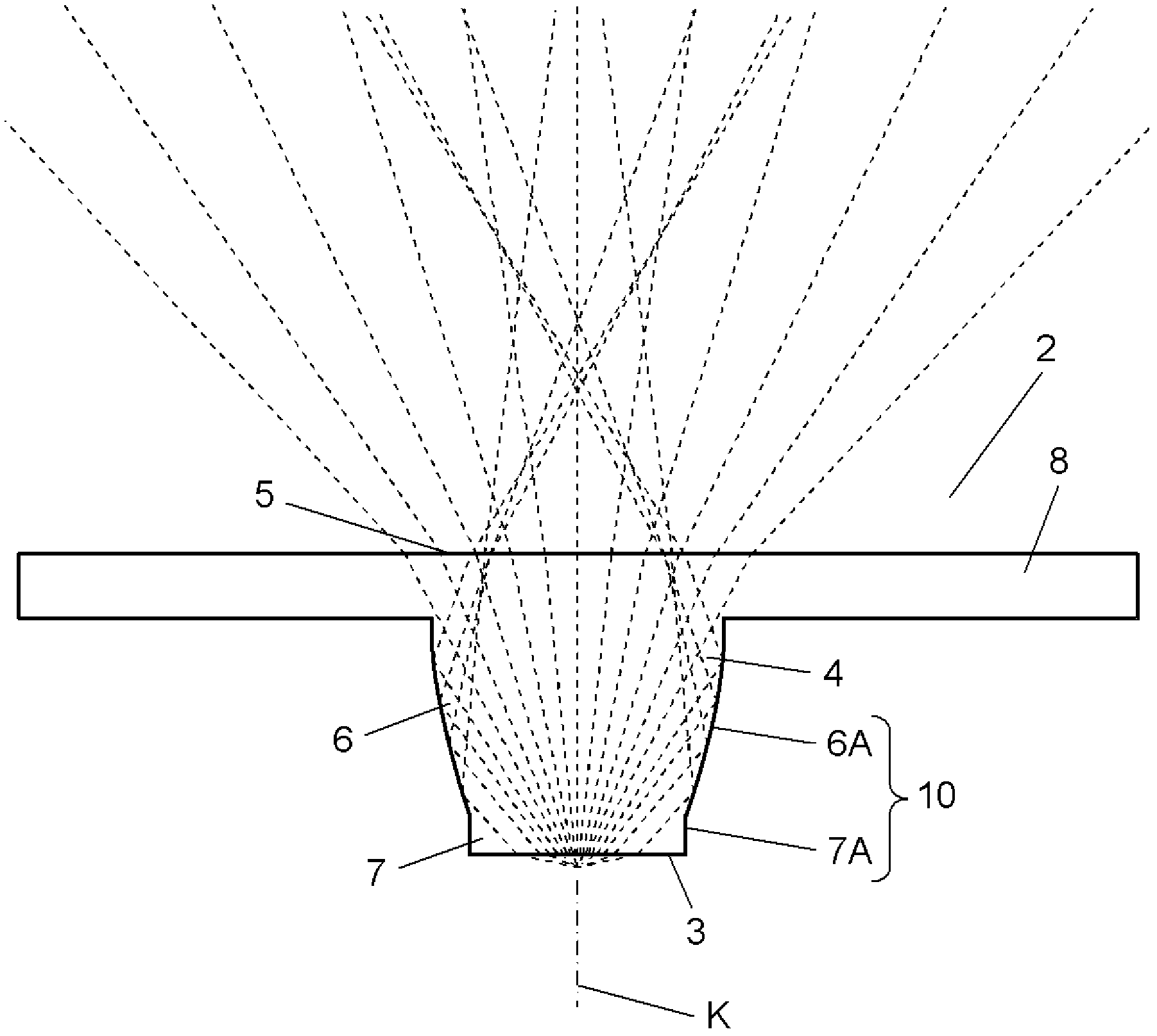
[0020] figure 1 It is an enlarged side view showing the structure of the semiconductor light emitting element module according to the embodiment of the present invention. figure 2 yes means figure 1 An explanatory diagram of the alignment of the lens of the semiconductor light emitting element module shown. Figure 3A , Figure 3B , Figure 3C respectively figure 2 Top view, left side view, front view of the lens shown. This semiconductor light emitting element module includes, for example, a light source (point light source) 1 composed of, for example, a light emitting diode (LED) mounted on a substrate (not shown), and a lens arranged in front of one side of the light emitting surface 1A of the light source 1. 2. The light source 1 composed of chip-type LEDs has a reflector. The shape of the reflector is circular in plan view, and may also be elliptical, square or polygonal. Such a semiconductor light emitting element module is incorporated in a mobile phone or the...
PUM
 Abstract
Description
Claims
Application Information
 - R&D Engineer
- R&D Manager
- IP Professional
- Industry Leading Data Capabilities
- Powerful AI technology
- Patent DNA Extraction
Browse by: Latest US Patents, China's latest patents, Technical Efficacy Thesaurus, Application Domain, Technology Topic, Popular Technical Reports.
© 2024 PatSnap. All rights reserved.Legal|Privacy policy|Modern Slavery Act Transparency Statement|Sitemap|About US| Contact US: help@patsnap.com