Through-wiring board and method of manufacturing same

A technology for wiring substrates and manufacturing methods, which is applied in the fields of printed circuit manufacturing, semiconductor/solid-state device manufacturing, semiconductor/solid-state device components, etc., and can solve problems such as narrowing of electrode intervals

Inactive Publication Date: 2012-05-23
THE FUJIKURA CABLE WORKS LTD
View PDF5 Cites 2 Cited by
  • Summary
  • Abstract
  • Description
  • Claims
  • Application Information

AI Technical Summary

Problems solved by technology

Also, when the number of electrodes on the surface of each device facing the substrate is large, the distance between the electrodes becomes narrower as the device becomes smaller.

Method used


Image

  • Through-wiring board and method of manufacturing same
  • Through-wiring board and method of manufacturing same
  • Through-wiring board and method of manufacturing same

Examples


Embodiment Construction

[0060] Hereinafter, embodiments of the present invention will be described with reference to the drawings.

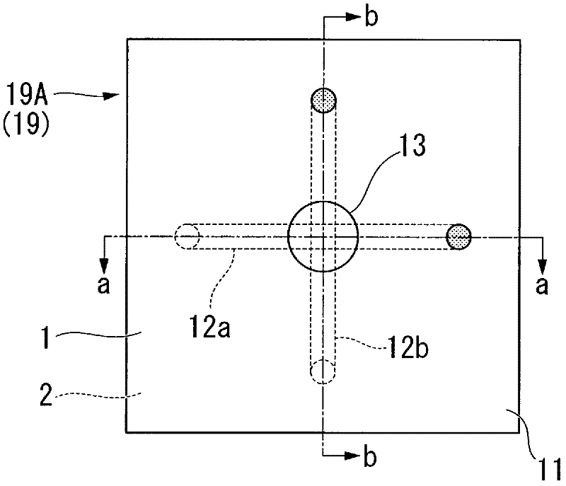
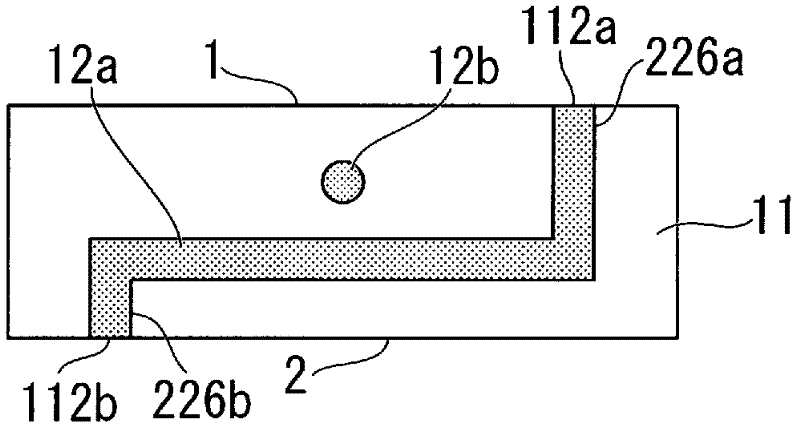
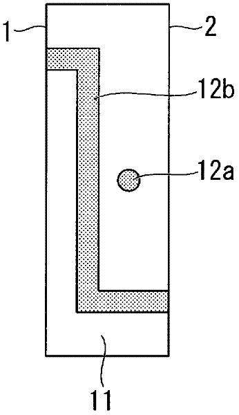
[0061] Figure 1A ~ Figure 6C It is a plan view and a cross-sectional view showing interposer substrate 19 according to the embodiment of the present invention. As shown in each drawing, through-wiring substrate 19 according to the embodiment of the present invention includes a plurality of through-wiring wirings penetrating through two or more surfaces constituting single substrate 11 . In addition, the through-wirings of each through-wiring substrate 19 are separated from each other, and have at least one overlap when viewed from the overlapping direction of the two surfaces (first surface and second surface) forming the front and rear surfaces of the substrate 11 . The overlapping portion 13 (intersection). That is, the through-wirings of the through-wiring substrate 19 are separated from each other, and at least one overlapping portion 13 is provided in plan view ...


PUM


Abstract

A through-wiring board comprising: a substrate provided with a first surface and a second surface; and lengths of through-wiring formed in through-holes, which penetrate between the first surface and the second surface, by filling an electrically conducting substance into the through-holes or by forming in the through-holes films of the electrically conducting substance. The lengths of through-wiring are separated from each other and each have, in a plan view of the substrate, at least one portion which overlaps with each other.

Description

technical field [0001] The present invention relates to a through-wiring substrate having a through-wiring that penetrates the inside of the substrate and a method of manufacturing the same. [0002] this application claims priority based on Japanese Patent Application No. 2009-164001 for which it applied to Japan on July 10, 2009, and uses the content here. Background technique [0003] Conventionally, as a method of electrically connecting a first device mounted on a first surface, which is one side of a substrate, and a second device mounted on a second surface, which is the other surface, a method of providing a through wiring penetrating through the inside of the substrate has been used. method. [0004] As an example of a through-wiring substrate, Patent Document 1 describes a through-wiring substrate having a through-wiring in which a conductive substance is filled into fine holes having a portion extending in a direction different from the thickness direction of the...

Claims


Application Information

Patent Timeline
Patent Type & Authority Applications(China)
IPC IPC(8): H05K1/11H01L23/36H05K1/02H05K3/00H05K3/40H01L21/768H01L23/12H01L23/522H01L25/07H01L25/18
CPCH05K2201/09981H01L21/486H01L23/49827H05K2201/09845H05K2201/09245H05K3/42H01L23/49822H05K3/101H05K1/0272H05K1/115H01L2924/09701H01L2924/0002H01L2924/00
Inventor 山本敏桥本广和
Owner THE FUJIKURA CABLE WORKS LTD
Why Eureka
Try Eureka