Super thick copper PCB plate production method and its circuit board

A manufacturing method and PCB board technology, applied in chemical/electrolytic methods to remove conductive materials, printed circuits, printed circuit manufacturing, etc., can solve the problem of high cumulative thickness, limited batch production, and no processing technology for products with a thickness of over 400 UM, etc. problem, to achieve the effect of uniform copper coating on the line and meet the basic requirements

Active Publication Date: 2012-06-20
SHENZHEN KINWONG ELECTRONICS
View PDF5 Cites 34 Cited by
  • Summary
  • Abstract
  • Description
  • Claims
  • Application Information

AI Technical Summary

Problems solved by technology

[0005] 1. Due to the use of photosensitive green oil for multiple printings on the surface of the circuit, because of the high cumulative thickness, it is easy to cause shrinkage and cracking of the surface photosensitive green oil when the heat resistance test is performed after the finished product, which affects the reliability of the PCB boar

Method used


Image

  • Super thick copper PCB plate production method and its circuit board
  • Super thick copper PCB plate production method and its circuit board

Examples


Embodiment Construction

[0031] Various preferred embodiments of the present invention will be described in more detail below in conjunction with the accompanying drawings.

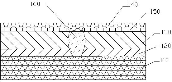
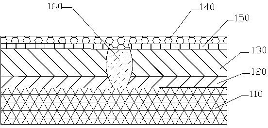
[0032] The ultra-thick copper PCB board manufacture method disclosed by the present invention and circuit board thereof, such as figure 1 As shown, it forms an ultra-thick PCB board. Specifically, on the substrate base material layer 110, the original copper clad layer is used as the bottom copper layer 120 with a thickness of 200um. Through continuous electroplating, it needs to be repeated many times. An electroplating thickening layer 130 is formed, and the thickness of the copper-clad circuit thereof exceeds 350 um, and is above 350-410 um. A circuit layer 150 and a green oil layer 140 are formed on the top of the circuit copper, and at the same time, epoxy resin 160 must be filled between the circuits to ensure the practical production process of the circuit board.

[0033] The basic process flow steps of the ultra-thick co...


PUM

PropertyMeasurementUnit
Thicknessaaaaaaaaaa
Thicknessaaaaaaaaaa

Abstract

The invention discloses a super thick copper PCB plate production method and its circuit board. The method comprises the following steps: dividing a plate substrate with a bottom copper; suspending and placing the PCB plate to be processed into an electroplating jar in a way of positive, negative clamping plates to electroplate the PCB plate for four times, until the thickness of the electroplating layer is more than 350-400Mum; etching the PCB plate; performing silk-screen printing using epoxy resin, leveling up circuit clearances by the epoxy resin and roasting the plate to solidify the epoxy resin; grinding the solidified epoxy resin and removing the residual resin layer on the surface of the circuit; drilling the plate, depositing the copper and electroplating the whole plate; performing the second time pattern electroplating and circuit etching on the plate to accomplish the circuit pattern. The super thick copper PCB plate production method and its circuit board use the multiple electroplating way and the epoxy resin leveling-up way between circuits, so as to realize the practical production technology of the super thick copper PCB plate, the copper on the circuit of the circuit board is uniform to satisfy the basis requirement of the circuit board.

Description

technical field [0001] The invention relates to a manufacturing process of a PCB board and a circuit board thereof, in particular to a method for manufacturing an ultra-thick copper PCB board and a circuit board device. Background technique [0002] In the prior art, with the continuous development and maturity of the consumer electronics market, more and more functional components are integrated on the PCB, and the requirements for the current conduction capacity and carrying capacity of the circuit are also very high; most of the heat needs to be (about 70%) into the circuit board, the heat has to be released through the circuit board itself, so the development of high-reliability ultra-thick copper foil printed board technology is difficult. [0003] At present, the copper thickness in the industry is generally about 200UM, and there is no thicker copper plate product, and when this type of circuit board is produced, the height difference between the base material and the...

Claims


Application Information

Patent Timeline
IPC IPC(8): H05K3/00H05K3/06H05K1/02
Inventor 谢伦魁何自立
Owner SHENZHEN KINWONG ELECTRONICS
Why Eureka
Try Eureka