Method for manufacturing PCB (Printed Circuit Board) with stepped grooves
A technology of PCB board and production method, which is applied in printed circuit manufacturing, electrical components, printed circuits and other directions, can solve the problems of high cost and high requirements for operating skills of silicone sheets, and achieve the effects of low cost, simple operation and high operation efficiency.
- Summary
- Abstract
- Description
- Claims
- Application Information
AI Technical Summary
Problems solved by technology
Method used
Image

Examples
Embodiment Construction
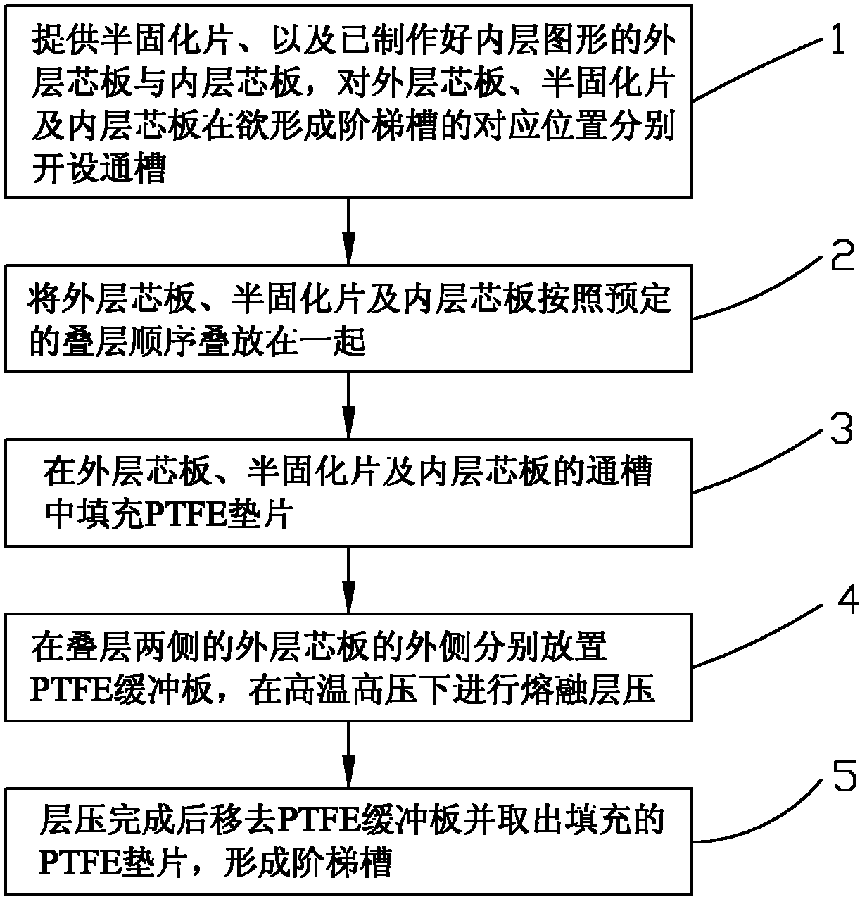
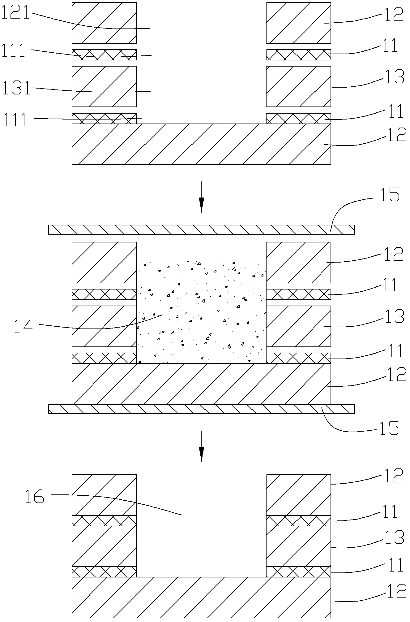
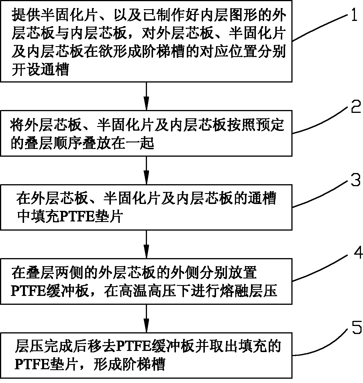
[0021] Such as figure 1 and figure 2 Shown, the manufacturing method of the PCB board of tool stepped groove of the present invention, comprises the following steps;
[0022] Step 1: Provide the prepreg 11, and the outer core board 12 and the inner core board 13 with the inner layer graphics already made, the outer core board 12, the prepreg 11 and the inner core board 13 are at the corresponding positions where the stepped groove 16 is to be formed Open through grooves 111, 121, 131 respectively;
[0023] Step 2: Stack the outer core board 12, the prepreg 11 and the inner core board 13 together according to the predetermined stacking sequence;
[0024] Step 3: Fill polytetrafluoroethylene (PTFE) gaskets 14 in the through grooves 111, 121, 131 of the outer core board 12, the prepreg 11 and the inner core board 13, and the PTFE gasket 14 can be processed by a milling machine become;
[0025] Step 4: Place PTFE buffer plates 15 on the outer sides of the outer core plates 12...
PUM
| Property | Measurement | Unit |
|---|---|---|
| Thickness | aaaaa | aaaaa |
Abstract
Description
Claims
Application Information
 - Generate Ideas
- Intellectual Property
- Life Sciences
- Materials
- Tech Scout
- Unparalleled Data Quality
- Higher Quality Content
- 60% Fewer Hallucinations
Browse by: Latest US Patents, China's latest patents, Technical Efficacy Thesaurus, Application Domain, Technology Topic, Popular Technical Reports.
© 2025 PatSnap. All rights reserved.Legal|Privacy policy|Modern Slavery Act Transparency Statement|Sitemap|About US| Contact US: help@patsnap.com