

Solid-state imaging device, semiconductor device, manufacturing methods thereof, and electronic apparatus
A technology for a camera device and a manufacturing method, which is applied in the fields of semiconductor/solid-state device manufacturing, semiconductor device, semiconductor/solid-state device components, etc., can solve the problems of difficulty in applying wafer-to-wafer bonding, increased cost, and difficulty in miniaturizing components, and achieves The effect of improving image quality, reducing the effects of electromagnetic waves or crosstalk
Active Publication Date: 2012-07-04
SONY CORP
View PDF7 Cites 22 Cited by
- Summary
- Abstract
- Description
- Claims
- Application Information
AI Technical Summary
Problems solved by technology
However, in this structure, there arise problems such as an increase in manufacturing steps and an increase in cost, problems such as difficulty in miniaturization of components, or problems such as difficulty in applying wafer-to-wafer bonding
Method used
View moreImage
Smart ImageViewing Examples

Examples
no. 1 example
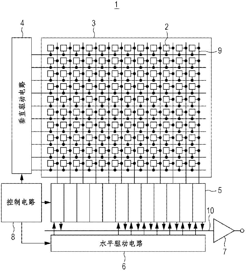
[0050] 1. First Embodiment: Backside Illuminated MOS Solid-State Imaging Device
[0051] 1-1. Overall structure
[0052] 1-2. Sectional structure of main parts
[0053] 1-3. Manufacturing method
[0054] 2. Second Embodiment: Backside Illuminated MOS Solid-State Imaging Device
no. 3 example
[0055] 3. Third Embodiment: Backside Illuminated MOS Solid-State Imaging Device
no. 4 example
[0056] 4. Fourth Embodiment: Backside Illuminated MOS Solid-State Imaging Device
Login to View More PUM
| Property | Measurement | Unit |
|---|---|---|
| Thickness | aaaaa | aaaaa |
| Thickness | aaaaa | aaaaa |
| Thickness | aaaaa | aaaaa |
Abstract
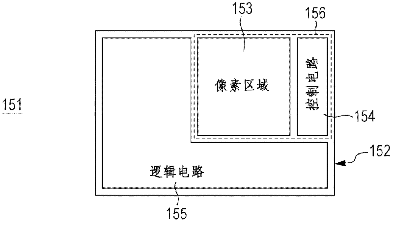
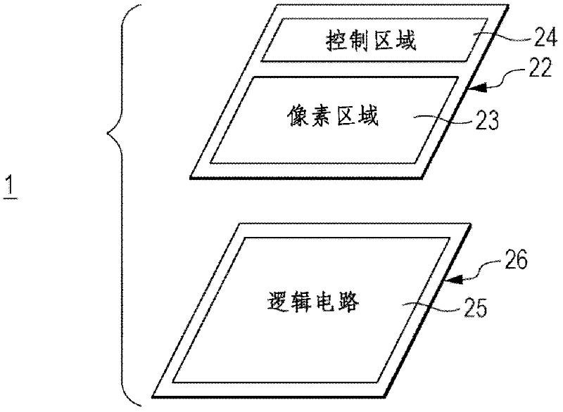
The invention relates to a solid-state imaging device, a semiconductor device, manufacturing methods thereof, and an electronic apparatus. The solid-state imaging device includes an imaging element and a logic element. The imaging element includes a first semiconductor substrate, a first wiring layer, and a first metal layer, in which a pixel region which is a light sensing surface is formed. The logic element includes a second semiconductor substrate, a second wiring layer, and a second metal layer, in which a signal processing circuit that processes a pixel signal obtained at the pixel region is formed. The logic element is laminated to the imaging element so that the first metal layer and the second metal layer are bonded to each other, and the first metal layer and the second metal layer are formed on a region excluding a region in which a penetrating electrode layer penetrating a bonding surface of the imaging element and the logic element is formed.
Description
[0001] Cross References to Related Applications [0002] The present application contains subject matter related to the disclosure of Japanese Priority Patent Application JP 2010-241491 filed in the Japan Patent Office on Oct. 27, 2010, the entire content of which is hereby incorporated by reference. technical field [0003] The present invention relates to a semiconductor device such as a solid-state imaging device and a method of manufacturing the same, and an electronic device such as a camera including the solid-state imaging device. Background technique [0004] In recent years, due to the high integration of LSI (Large Scale Integration), miniaturization and multilayering of internal wiring have been developed. However, the high cost of semiconductor manufacturing devices due to miniaturization greatly affects the cost of LSIs. In addition, a method of mixing and arranging logic circuits, memories, imaging devices, and the like on a single chip is also performed. How...
Claims
Login to View More Application Information
Patent Timeline
 IPC IPC(8): H01L27/146H01L23/552H04N5/374
CPCH01L27/1464H01L27/14627H01L27/14621H01L23/552H01L25/0657H01L27/14634H05K9/00H01L27/14636H01L2924/0002H01L2225/06513H01L2225/06541H01L21/76898H01L27/1469H01L23/481H01L2924/00H01L27/146
Inventor前田圭一
OwnerSONY CORP