Output buffer circuit

A technology for output buffering and circuits, applied in the direction of logic circuit connection/interface layout, logic circuit coupling/interface using field effect transistors, instruments, etc., which can solve problems such as device damage and overvoltage

Active Publication Date: 2013-11-06
SHANGHAI BEILING
View PDF5 Cites 0 Cited by
  • Summary
  • Abstract
  • Description
  • Claims
  • Application Information

AI Technical Summary

Problems solved by technology

[0014] In order to solve the above-mentioned problems in the prior art, the present invention aims to provide an output buffer circuit to overcome the problem of device damage caused by excessive gate-source and gate-substrate voltages of high-voltage devices in the BCD process, so that the output buffer circuit Can work normally under BCD process

Method used


Image

  • Output buffer circuit
  • Output buffer circuit
  • Output buffer circuit

Examples


Embodiment Construction

[0027] Specific embodiments of the present invention will be described in detail below in conjunction with the accompanying drawings.

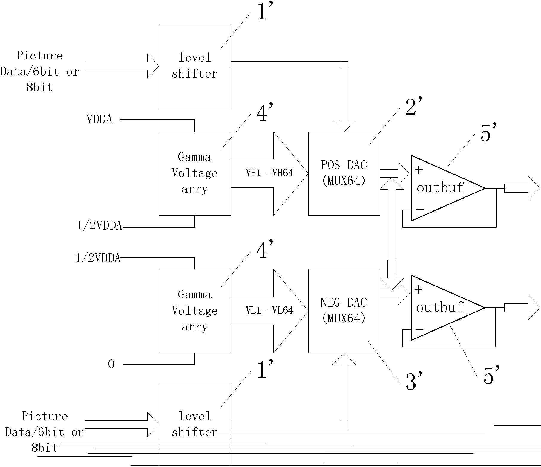
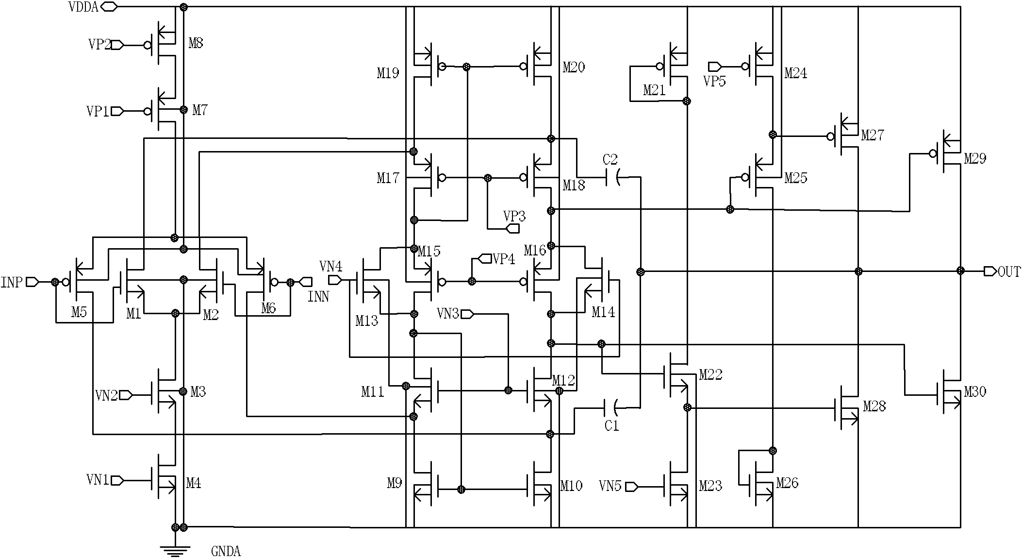
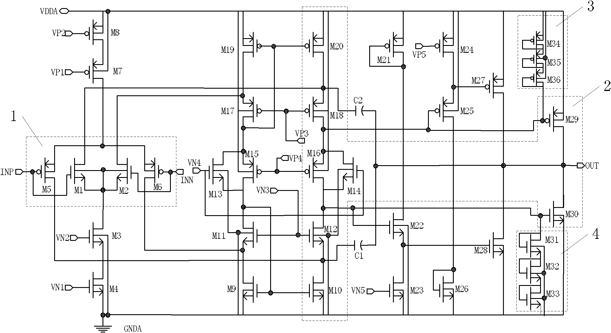
[0028] Such as image 3 As shown, the present invention is an output buffer circuit, which includes a rail-to-rail input module 1 , an AB output module 2 , a first voltage clamping module 3 and a second voltage clamping module 4 .

[0029] The rail-to-rail input module 1 is connected between the external power supply VDDA and the ground GNDA, and it includes a first MOS transistor M1, a second MOS transistor M2, a fifth MOS transistor M5 and a sixth MOS transistor M6, wherein,

[0030] The substrate of the fifth MOS transistor M5 is connected to the source, the substrate of the sixth MOS transistor M6 is connected to the source, and the sources of the fifth and sixth MOS transistors M5 and M6 are connected, and their gates respectively receive a positive voltage. Input voltage INP and a negative input voltage INN, the substrates and sources o...


PUM


Abstract

The invention relates to an output buffer circuit which comprises a rail-to-rail input module, an AB-type output module, a first voltage clamp module and a second voltage clamp module, wherein the rail-to-rail input module is connected in series between an external power supply and the ground; the AB-type output module is connected with the rail-to-rail input module; a source electrode of a fifth MOS (Metal Oxide Semiconductor) pipe is connected with a substrate; a source electrode of a sixth MOS pipe is connected with the substrate; a source electrode of a first MOS pipe is connected with the substrate; a source electrode of a second MOS pipe is connected with the substrate; the first voltage clamp module is connected between the external power supply and a grid electrode of a twenty-ninth MOS pipe; and the second voltage clamp module is connected between a grid electrode of a thirtieth MOS pipe and the ground. According to the invention, the source electrodes of the first, second, fifth and sixth MOS pipes are respectively in short connection with the substrate, so that gate sources and gate linings of the first, second, fifth and sixth MOS pipes are ensured not to be broken down under a certain limited current; and moreover, the first and second voltage clamp modules are respectively added into the grid electrodes of the twenty-ninth and thirtieth MOS pipes, so that the grid electrodes of the twenty-ninth and thirtieth MOS pipes are ensured not to be broken down.

Description

technical field [0001] The invention relates to an integrated circuit, in particular to an output buffer circuit for a column driver circuit developed based on a BCD process (a monolithic integration process for making bipolar, CMOS and DMOS devices on the same chip). Background technique [0002] In the column drive circuit (Source Driver) used for large-scale TFT-LCD screens, when the HV (High Voltage, high voltage) CMOS process is used for development, the threshold voltage of the MOS transistor provided by this process is large, the transconductance is small, and the conductance The on-resistance is large, so for large load applications, the area of ​​the output circuit will be relatively large. In order to solve the above problems, people in the industry began to use the characteristics of large transconductance and small on-resistance of LDMOS devices in the BCD process to develop column drive circuits for large-size TFT-LCD screens based on the BCD process, thereby re...

Claims


Application Information

Patent Timeline
Patent Type & Authority Patents(China)
IPC IPC(8): H03K19/0185G09G3/20G09G3/36
Inventor 覃正才吴大军李冠林李长虹张建玲刘启付吕回周承捷
Owner SHANGHAI BEILING
Why Eureka
Try Eureka