Transfer box for cleaning of silicon wafers

A silicon wafer cleaning and turnover box technology, which is applied in the directions of cleaning methods and utensils, chemical instruments and methods, etc., can solve the problems of easy slipping of silicon wafers, insufficiency of taking and placing silicon wafers, high pressure on silicon wafers, etc. Putting operation, reducing the chance of fragmentation, and high work efficiency

Inactive Publication Date: 2012-07-11
KONCA SOLAR CELL
View PDF10 Cites 4 Cited by
  • Summary
  • Abstract
  • Description
  • Claims
  • Application Information

AI Technical Summary

Problems solved by technology

[0003] The purpose of the present invention is to solve the above problems and provide a silicon wafer cleaning turnover box to solve the problem that the traditional silicon wafer cleaning turnover box does not take and place silicon wafers all over the place, and the line contact stacking produces a large pressure on

Method used


Image

  • Transfer box for cleaning of silicon wafers
  • Transfer box for cleaning of silicon wafers
  • Transfer box for cleaning of silicon wafers

Examples


Embodiment Construction

[0015] The technical solutions of the present invention will be further described below in conjunction with the accompanying drawings and through specific implementation methods.

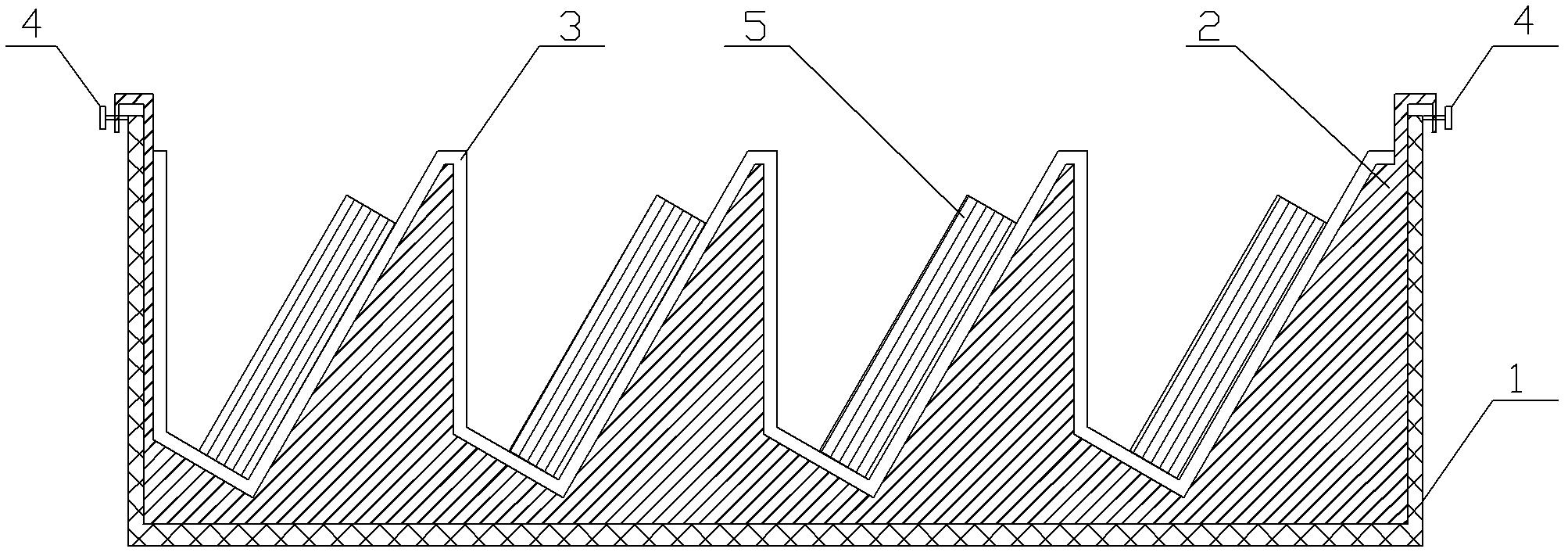
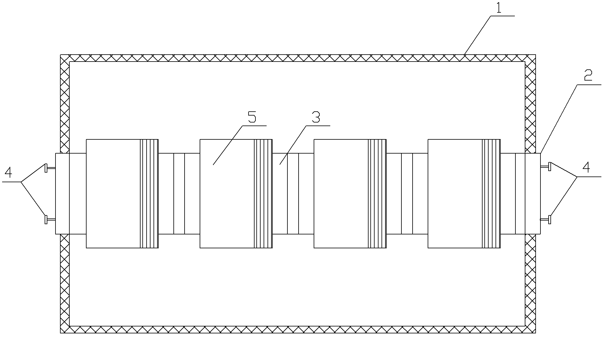
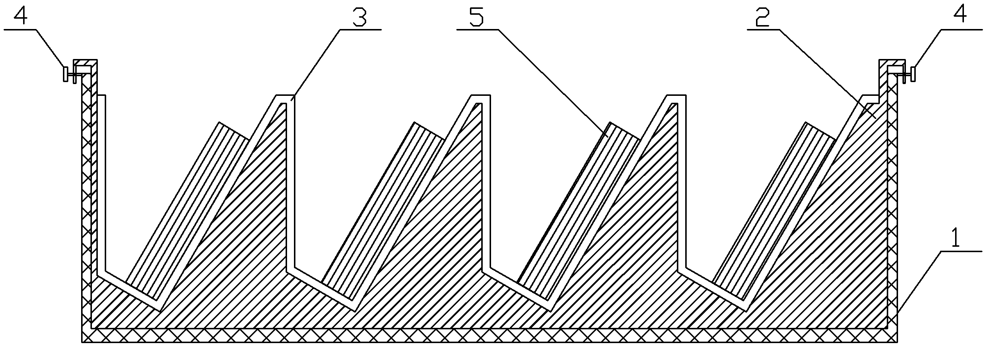
[0016] Please refer to figure 1 and figure 2 As shown, in this embodiment, a silicon wafer cleaning turnover box includes a box body 1, the box body 1 is a rectangular structure, made of plastic, and a bracket 2 is detachably arranged in it, and the bracket The frame 2 has four V-shaped grooves for placing the silicon wafer 5, and the width of the bracket 2 is smaller than the width of the silicon wafer 5, and its surface is covered with a rubber pad 3 for anti-skid and shock absorption.

[0017] In actual use, the bracket 2 is first fixed in the box body 1 by bolts 4, and then the box body 1 is filled with water. When placing the silicon wafer 5, the silicon wafer 5 can be gently placed on the rubber pad 3 in the V-shaped groove on the bracket 2, and the center line of the silicon wafer 5 is bas...


PUM


Abstract

The invention discloses a transfer box for cleaning of silicon wafers, which comprises a box body. A support is arranged in the box body and provided with at least one V-shaped groove for holding silicon wafers. By the aid of the transfer box for cleaning of silicon wafers, the silicon wafers can be stored and picked conveniently. A rubber pad covering the surface of the support is capable of reducing impact and pressure subjected by the silicon wafers when the silicon wafers are stored and picked, and sliding of the silicon wafers is avoided effectively and the breakage probability of the silicon wafers is lowered due to the design of the V-shaped grooves on the support. The width of the support is smaller than that of the silicon wafers and gripping spaces can be reserved on two sides of silicon wafers on the support, so that the silicon wafers can be stored and picked conveniently. In addition, due to the fact that the support is detachable, silicon dust left on the surface of the support can be cleaned directly without changing of water in the box body, then damages to the edges of the silicon wafers caused by silicon chips can be reduced, and high work efficiency can be achieved.

Description

technical field [0001] The invention relates to a silicon wafer cleaning auxiliary tool, in particular to a silicon wafer cleaning turnover box. Background technique [0002] At present, the silicon wafer cleaning turnover box is an auxiliary tool used for temporarily storing degummed silicon wafers during the silicon wafer cleaning process. The existing silicon wafer cleaning turnover box is a rectangular plastic box. When using it, fill the plastic box with water, then directly put the degummed silicon wafers into the box vertically, and lean one side of the silicon wafer against the edge of the plastic box. On the inner side, the silicon chips are in line contact with the inner side of the edge of the plastic box. This structure can still be used with a small number of stacked silicon chips. On the silicon chip on the inside of the edge of the plastic box, it is easy to cause the silicon chip to break. Simultaneously, because the bottom of the plastic box is relatively ...

Claims


Application Information

Patent Timeline
IPC IPC(8): B08B13/00
Inventor 王秦伟蔺雷亭王欣何晋康
Owner KONCA SOLAR CELL
Why Eureka
Try Eureka