Organic light-emitting diode (LED) pixel circuit and display device

A technology of light-emitting diodes and pixel circuits, applied in static indicators, instruments, etc., can solve the problems of Id drift, change of Id, and deterioration of OLED display effect, and achieve the effect of reducing the amount of change and improving the change of display effect

Active Publication Date: 2012-07-11
SHANGHAI TIANMA MICRO ELECTRONICS CO LTD
View PDF5 Cites 26 Cited by
  • Summary
  • Abstract
  • Description
  • Claims
  • Application Information

AI Technical Summary

Problems solved by technology

[0006] However, the defect of the organic light emitting diode pixel (2T1C structure) circuit in the prior art is that in practical applications, due to the influence of manufacturing process and other conditions, the carrier mobility u and the threshold voltage Vth will inevitably drift to a certain extent, The pixel power supply voltage VDD will also be affected by the voltage drop on the line because of the current flowing through it; these will change the value of Id, causing Id to drift, thereby deteriorating the display effect of OLED

Method used


Image

  • Organic light-emitting diode (LED) pixel circuit and display device
  • Organic light-emitting diode (LED) pixel circuit and display device
  • Organic light-emitting diode (LED) pixel circuit and display device

Examples


Embodiment 1

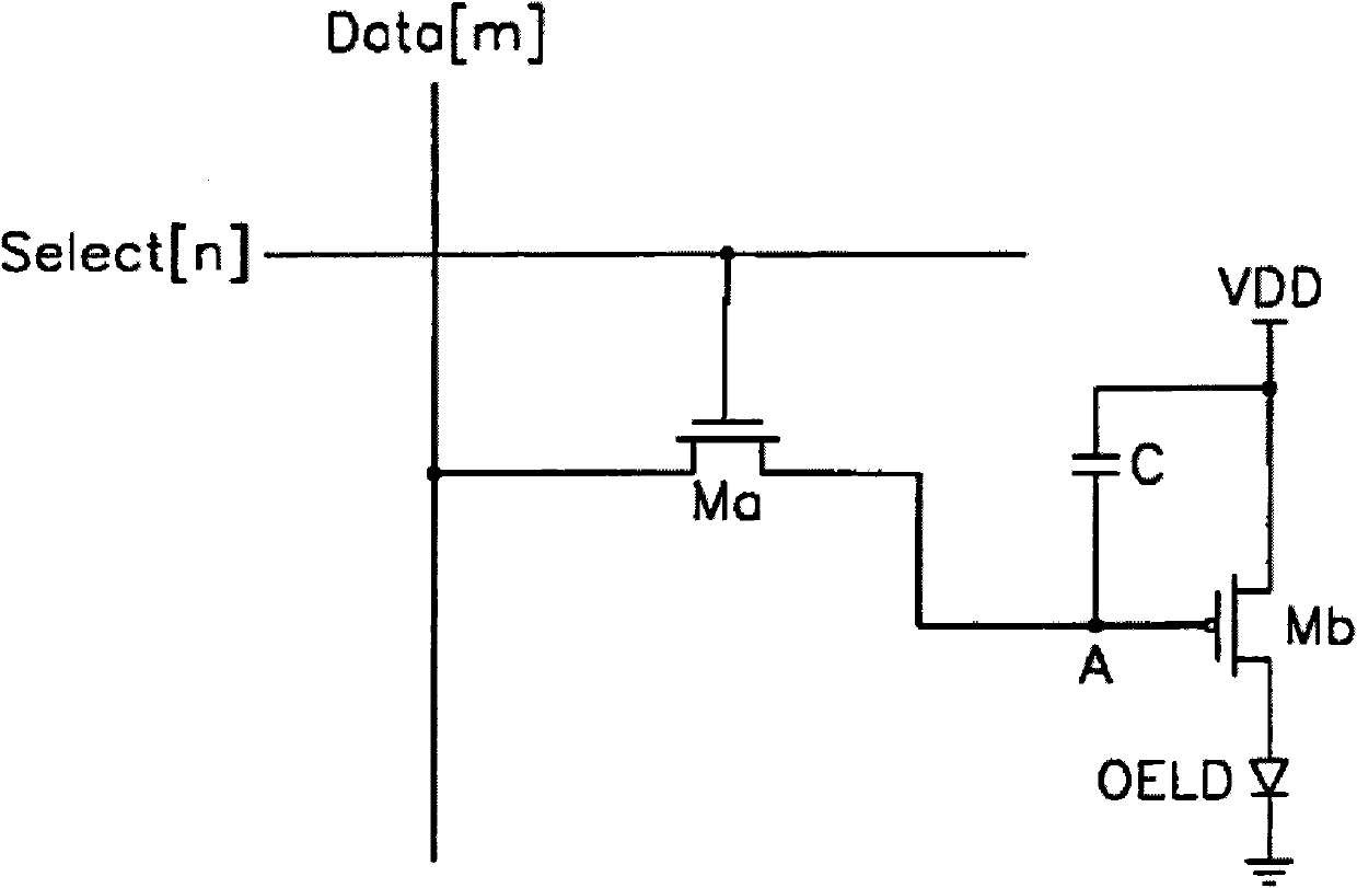
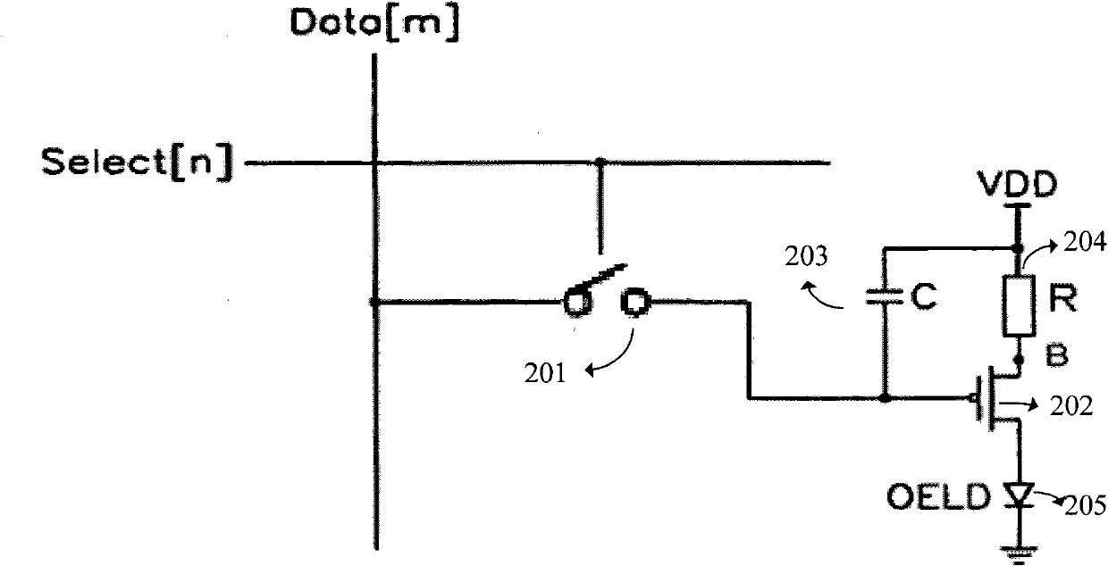
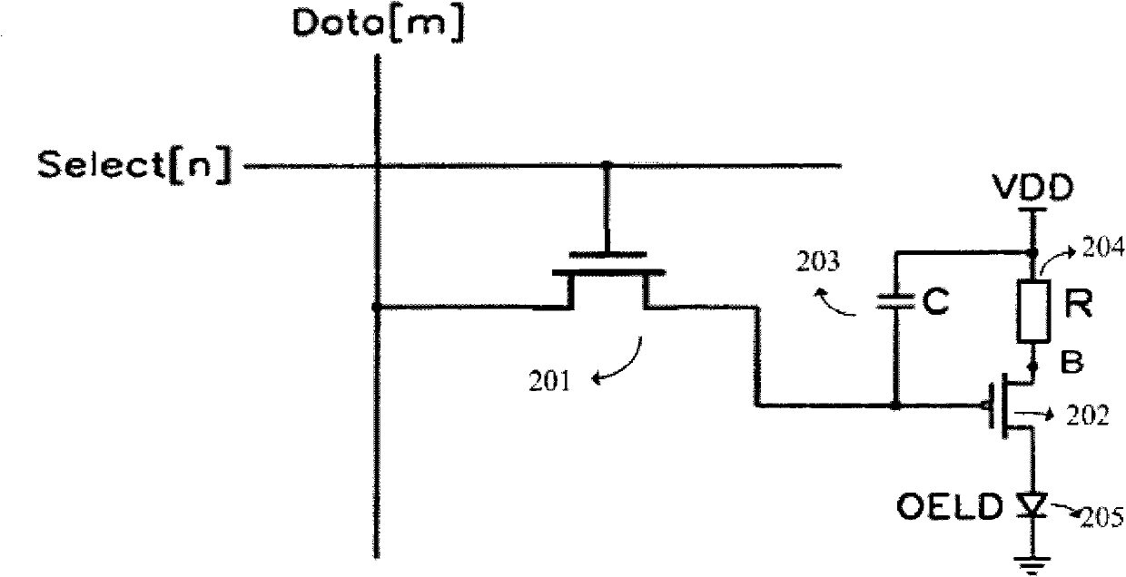
[0029] figure 2 It is a schematic structural diagram of an organic light emitting diode pixel circuit provided by Embodiment 1 of the present invention. Such as figure 2 As shown, the scan line Select[n] and the data line Data[m] define the pixel area of ​​the OLED pixel. The switch element 201 is connected between the data line Data[m] and the gate of the driving transistor 202, and the switch state of the switch element 201 is determined according to the control signal of the scan line Select[n]. When the switch element 201 is turned on, the data signal on the data line Data[m] is transmitted to the gate of the driving transistor 202 to control the switching of the driving transistor 202 . The driving transistor 202 is a P-type transistor, generally a P-type TFT. The source of the drive transistor 202 is connected to the pixel power supply VDD through a resistor R204, and its drain is connected to the anode of the OLED205; the cathode of the OLED205 is connected to a fi...

Embodiment 2

[0048] The working principle of the OLED pixel circuit provided in Embodiment 2 is similar to that of the OLED pixel circuit provided in Embodiment 1, and will not be repeated here.

[0049] The present invention also provides a display device, which includes the organic light emitting diode pixel circuit provided in the first embodiment or the second embodiment.

[0050] It can be seen from the above embodiments that by adding a resistor, the voltage of the transistor in the organic light emitting diode pixel circuit can change with the drift of Id, and feed back to the transistor, thereby reducing the amount of change in Id, that is, suppressing the change in Id, and improving The change of display effect caused by current drift.


PUM


Abstract

The invention provides an organic light-emitting diode (LED) pixel circuit and a display device. The organic LED pixel circuit comprises an organic LED, a drive transistor and a resistor, wherein the organic LED is driven to emit light by the source drain current of the drive transistor; the resistor is coupled to a source electrode of the drive transistor, and is used for restraining the change of the source drain current through changing the voltage of the drive transistor when the strength of the source drain current is changed. According to the organic LED pixel circuit and the display device, the resistor is additionally arranged on the source electrode of the drive transistor in the organic LED pixel circuit, so that the voltage of the drive transistor can be changed along with the drift of the current Id, and is fed back to the drive transistor, thereby, the variation of the current Id is reduced, and the condition that a display effect is changed because of current drift is improved.

Description

technical field [0001] The invention relates to the field of Active Matrix Organic Emitting Diode (AMOLED, Active Matrix Organic Emitting Diode), in particular to an organic light emitting diode pixel circuit and a display device. Background technique [0002] With the continuous improvement of active organic light emitting diode (AMOLED) technology, its advantages such as wide viewing angle, good color contrast effect, fast response speed and low cost have become more and more obvious, and it has been favored by more and more flat panel displays (FlatPanelDisplay) in the display field. manufacturer's attention. Therefore, AMOLED displays have become the focus of the display industry. [0003] The AMOLED can be equivalent to a diode, and by controlling the current of an organic light emitting diode (OLED, Organic Emitting Diode), the brightness can be controlled to display gray scales. Due to the driving characteristics of OLED, most OLED pixel circuits have a 2T1C structu...

Claims


Application Information

Patent Timeline
IPC IPC(8): G09G3/32G09G3/3233
Inventor 曾章和钱栋顾寒昱
Owner SHANGHAI TIANMA MICRO ELECTRONICS CO LTD
Why Eureka
Try Eureka