
Method for manufacturing strain semiconductor device structure

A device structure and semiconductor technology, which is applied in semiconductor/solid-state device manufacturing, electrical components, circuits, etc., can solve the problem of PMOS transistor saturation current decrease, and achieve the goal of preventing the increase of Miller capacitance, suppressing adverse effects, and suppressing saturation current Effect

Active Publication Date: 2012-07-11
SEMICON MFG INT (SHANGHAI) CORP +1
View PDF4 Cites 3 Cited by
  • Summary
  • Abstract
  • Description
  • Claims
  • Application Information

AI Technical Summary

Problems solved by technology

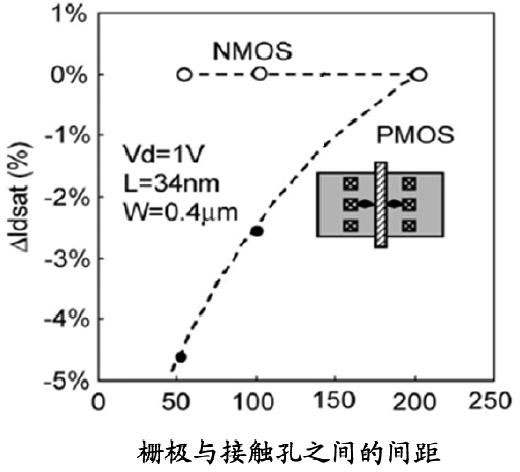
[0008] from figure 1 It can be seen that the saturation current of the PMOS transistor is significantly reduced after being processed by the existing comprehensive SPT technology.

Method used

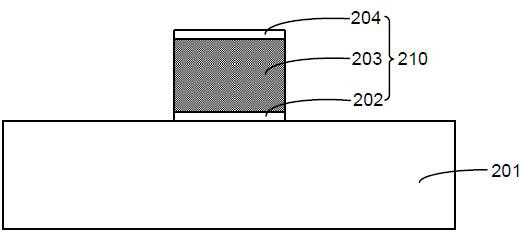
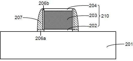

Image

  • Method for manufacturing strain semiconductor device structure
  • Method for manufacturing strain semiconductor device structure
  • Method for manufacturing strain semiconductor device structure

Examples


Embodiment Construction

[0035] In the following description, numerous specific details are given in order to provide a more thorough understanding of the present invention. It will be apparent, however, to one skilled in the art that the present invention may be practiced without one or more of these details. In other examples, some technical features known in the art are not described in order to avoid confusion with the present invention.

[0036] In order to thoroughly understand the present invention, detailed steps will be presented in the following description to illustrate how the present invention fabricates the strained semiconductor device structure. Obviously, the practice of the invention is not limited to specific details familiar to those skilled in the semiconductor arts. Preferred embodiments of the present invention are described in detail below, however, the present invention may have other embodiments besides these detailed descriptions.

[0037] It should be noted that the terms...


PUM

PropertyMeasurementUnit
Thicknessaaaaaaaaaa
Thicknessaaaaaaaaaa

Abstract

The invention provides a method for manufacturing a strain semiconductor device structure. The method comprises the following steps of: providing a front end device structure, which comprises a semiconductor substrate and a grid structure positioned on the semiconductor substrate; forming a partially-ashable interval wall structure which is positioned on both sides of the grid structure and clings to the grid structure on the semiconductor substrate, wherein the partially-ashable interval wall structure comprises a first interval wall layer and a second interval wall layer in sequence from inside to outside; forming protective oxide layers on the surface of the semiconductor substrate, the surface of the partially-ashable interval wall structure and the surface of the grid structure; performing ion injection to form a source / drain region in the semiconductor substrate; removing the protective oxide layers and the second interval wall layer till the surface of the first interval wall layer is exposed; and forming strain introducing liner layers on the surface of the semiconductor substrate, the surface of the first interval wall layer and the surface of the grid structure. According to the method, adverse influences of SPT (Shortest Processing Time) processing on saturated current of a PMOS (P-channel Metal Oxide Semiconductor) transistor can be effectively suppressed, and damages to a siliconization region are avoided.

Description

technical field [0001] The present invention relates to semiconductor manufacturing processes, and in particular, to a method for fabricating strained semiconductor device structures. Background technique [0002] At present, the main factor affecting the performance of field effect transistors is the mobility of carriers, where the mobility of carriers will affect the magnitude of the current in the channel. The reduction in carrier mobility in field-effect transistors not only reduces the switching speed of the transistor, but also reduces the difference in resistance between on and off. Therefore, in the development of complementary metal-oxide-semiconductor field-effect transistors (CMOS), effectively improving carrier mobility has always been one of the key points in transistor structure design. [0003] Conventionally, P-type metal-oxide-semiconductor field-effect transistors (PMOS) and N-type metal-oxide-semiconductor field-effect transistors (NMOS) are treated separ...

Claims


Application Information

Patent Timeline
IPC IPC(8): H01L21/336H01L21/311
Inventor 张海洋胡敏达
Owner SEMICON MFG INT (SHANGHAI) CORP
Learn More