Semiconductor device
A semiconductor, N-type semiconductor technology, applied in the direction of semiconductor devices, electrical components, circuits, etc., can solve the problem of miniaturization limit and other problems, and achieve the effect of suppressing saturation current
- Summary
- Abstract
- Description
- Claims
- Application Information
AI Technical Summary
Problems solved by technology
Method used
Image
Examples
Embodiment approach 1
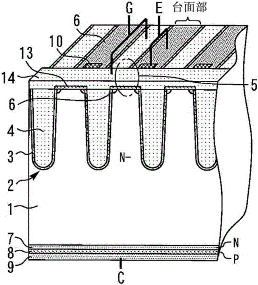
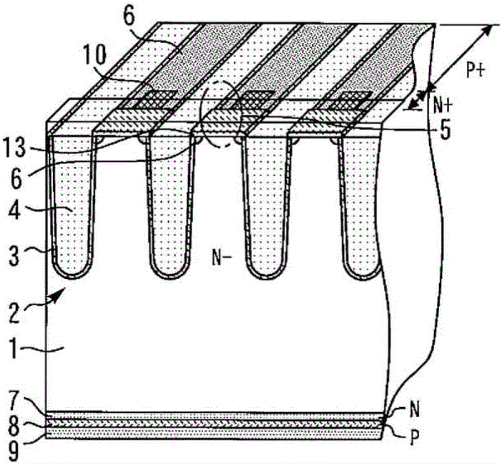
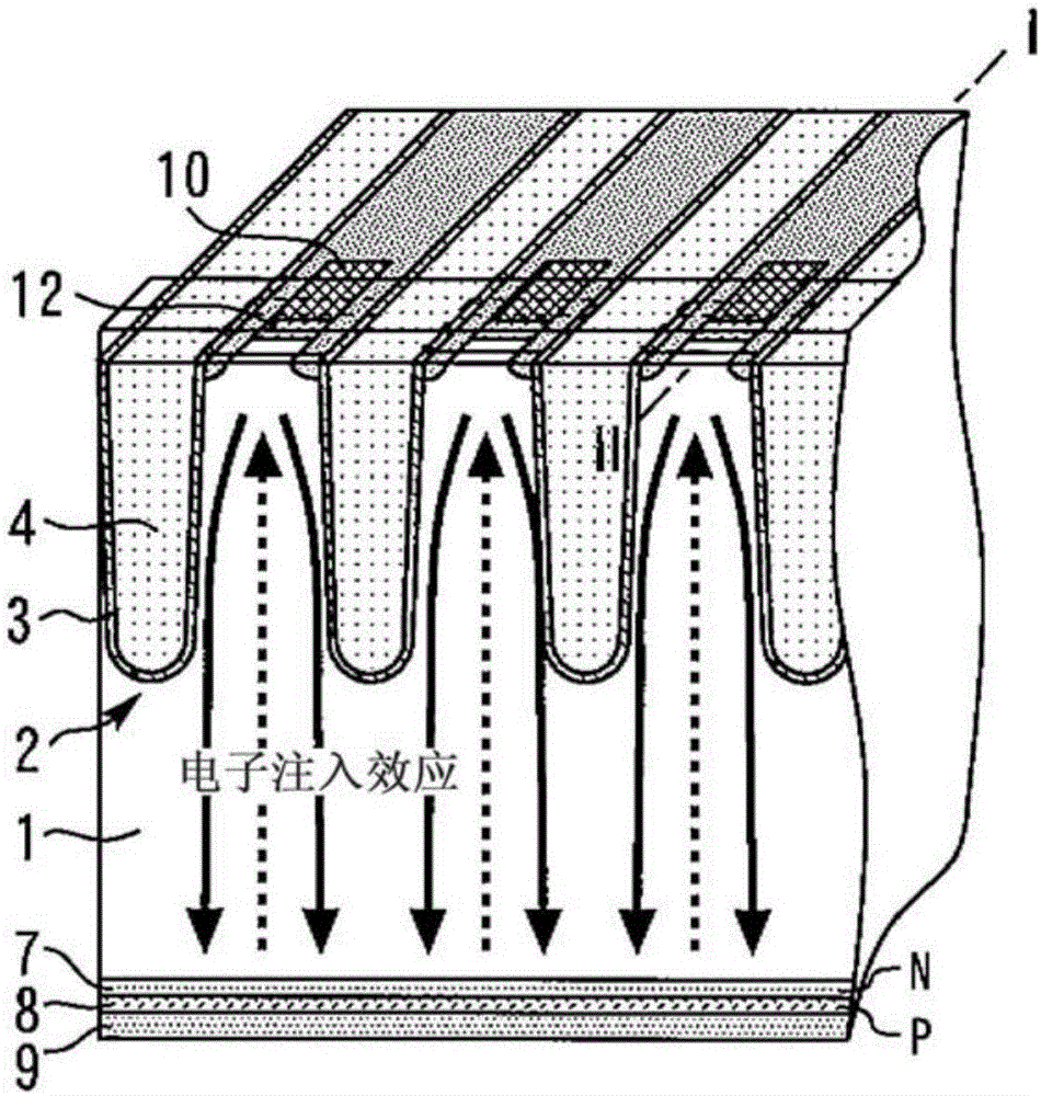
[0039] figure 1 It is a sectional perspective view showing the semiconductor device according to Embodiment 1 of the present invention. figure 2 is in figure 1 The cross-sectional oblique view after omitting the planar gate in the device. image 3 is in figure 1 The cross-sectional oblique view of the device in which the planar gate and gate insulating film are omitted. Figure 4 is along image 3 Sectional view of I-II. In addition, a high withstand voltage class of 6500V was shown in an example as an embodiment, but the present invention can be applied regardless of the withstand voltage class.
[0040] in N - The upper surface of the type semiconductor substrate 1 is provided with a plurality of trenches 2 . A gate trench 4 is provided in the trench 2 via an insulating film 3 . At the mesa portion between trench 2, at N - A planar MOSFET (Metal-Oxide-Semiconductor Field-Effect Transistor) 5 is provided on the upper surface of a type semiconductor substrate 1 . At...
Embodiment approach 2
[0055] Figure 14 It is a cross-sectional perspective view showing a semiconductor device according to Embodiment 2 of the present invention. Figure 15 is along Figure 14 Sectional view of I-II. The N-type diffusion layer 19 serving as the drain of the planar MOSFET 5 is provided over the entire cell region. N-type diffusion layer 19 and N - type semiconductor substrate 1 connection, with a ratio N - Type semiconductor substrate 1 has a high impurity concentration, and the depth is shallower than that of trench 2 . The N-type diffusion layer 19 serves as a hole blocking layer, and the carrier concentration on the emitter side of the device is increased, so that the on-voltage can be reduced. Other configurations and effects are the same as those of Embodiment 1.
Embodiment approach 3
[0057] Figure 16 It is a cross-sectional view showing a semiconductor device according to Embodiment 3 of the present invention. An N-type diffusion layer 19 is partially provided under the planar gate 14 . The other structures are the same as those in Embodiment 2. Also in this case, the same effects as in Embodiment 2 can be obtained.
[0058] Figure 17 It is a graph showing the conduction voltage of the semiconductor device according to Comparative Example 1 and Embodiments 1 to 3. The evaluation condition is V GE =15V,J C = Rated current density, T j = 25°C. It can be seen that, compared with the first embodiment, the on-state voltage is further lowered in the second and third embodiments.
PUM
| Property | Measurement | Unit |
|---|---|---|
| Length | aaaaa | aaaaa |
Abstract
Description
Claims
Application Information


