High-Aspect-Ratio Microdevices and Methods for Transdermal Delivery and Sampling of Active Substances

a micro-device and high-aspect ratio technology, applied in the field of high-aspectratio micro-devices, to achieve the effects of improving selectivity, minimally invasive, and increasing needle length

Active Publication Date: 2005-11-24
XU BAI
View PDF40 Cites 174 Cited by
  • Summary
  • Abstract
  • Description
  • Claims
  • Application Information

AI Technical Summary

Benefits of technology

[0012] Another object of the present invention is to fabricate high-aspect ratio microneedles with increased needle length and sensors are placed in the vicinity of microneedle base, leading to a minimally-invasive diagnostic system. S

Problems solved by technology

It's unobvious that solid microneedle, solid microblades and solid microknives can be practically usable to deliver ther

Method used


Image

  • High-Aspect-Ratio Microdevices and Methods for Transdermal Delivery and Sampling of Active Substances
  • High-Aspect-Ratio Microdevices and Methods for Transdermal Delivery and Sampling of Active Substances
  • High-Aspect-Ratio Microdevices and Methods for Transdermal Delivery and Sampling of Active Substances

Examples


example 1

[0065] Fabrication of Si Microneedles

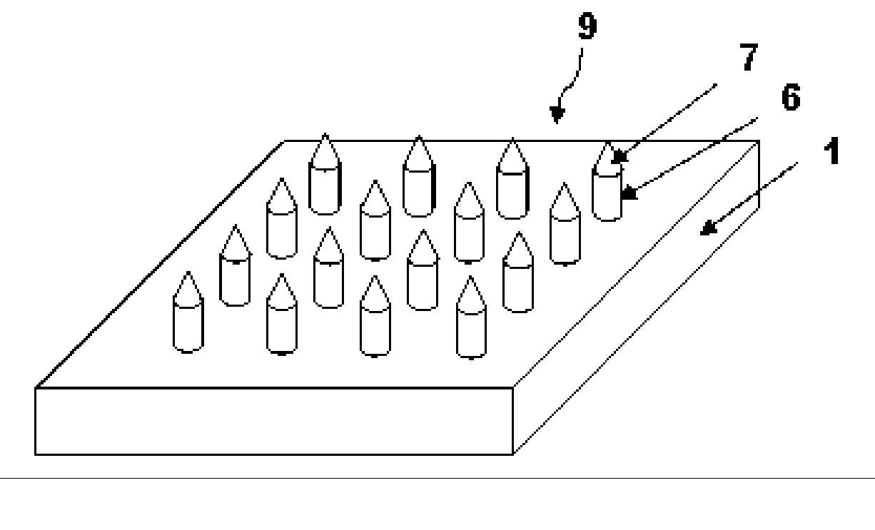
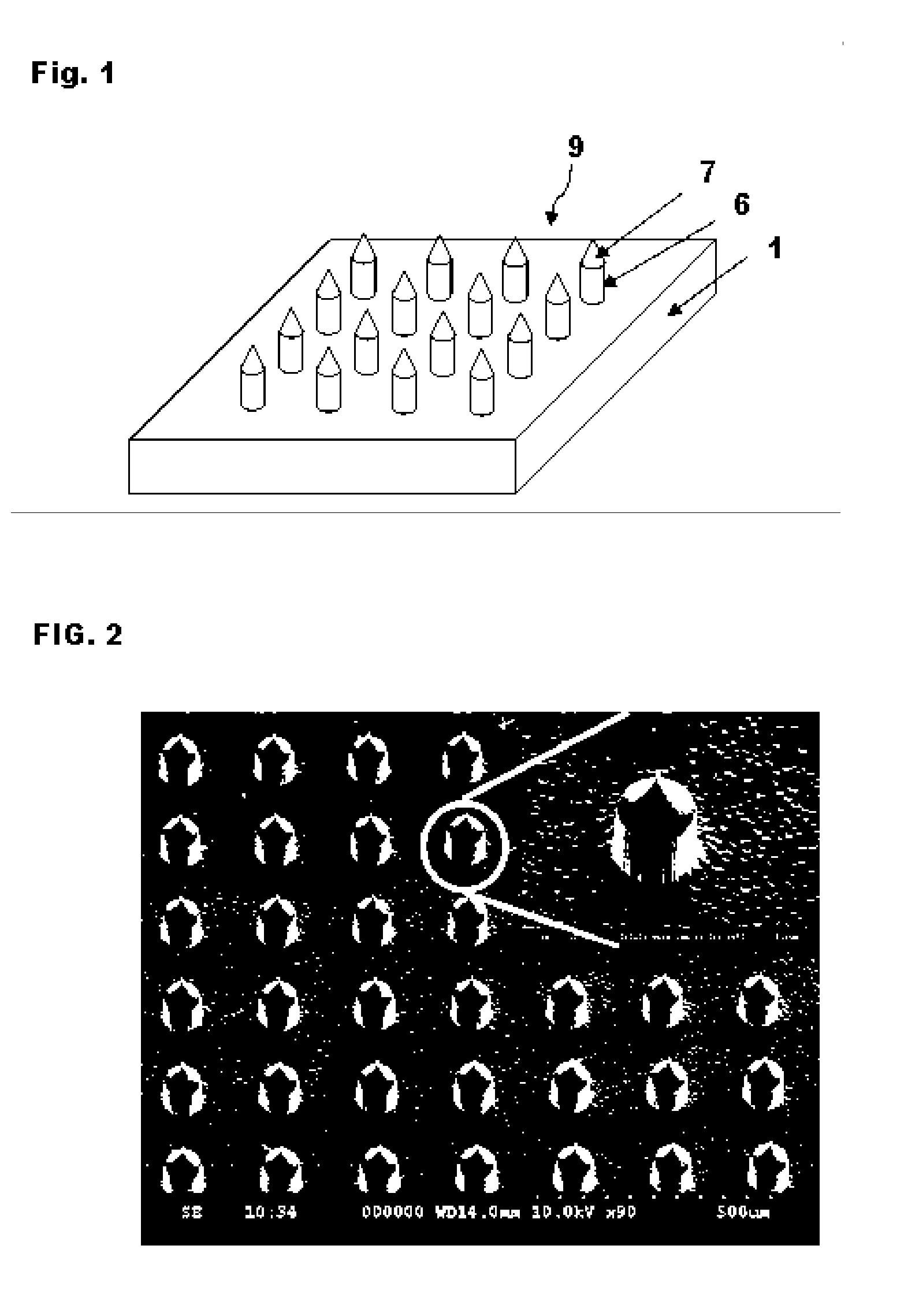
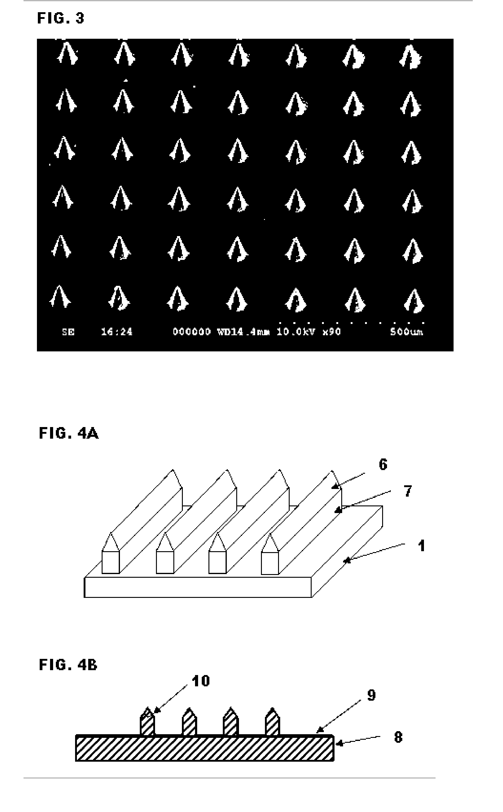
[0066] Bosch etch process is a widely used MEMS process that is known in the art to etch deep vias and trenches. The current invention disclosed a method that involved isotropic etch first to form microneedle tip 6 and second anisotropic Bosch etch later to form microneedle shaft 7 as shown in FIG. 6G.

[0067] Referring to FIG. 6A, a silicon wafer 1 of any crystal orientation with about 1 micron of thermal oxide 2 coated on both sides was used as substrate. Doping level in the silicon substrate was found to be not critical. A chromium layer with thickness ranging between 0.2 to 20 nm was sputtered onto the substrate. A layer of photoreist 3 was applied to front side of the wafer as shown in FIG. 6B. It was patterned into a number of circular islands with a diameter that was equal to the base of the microneedles as shown in FIG. 6C. The shape of the pattern was changed to rectangular to form microknives and microblades. The Cr etch was done using ...

example 2

[0068] Fabrication of Si Microneedles

[0069] The current invention also disclosed a method that did anisotropic etch first to form microneedle body and switch to orientation dependent etch (ODE) later to form microneedle shaft and tip.

[0070] A silicon wafer of orientation with 0.5-3 micron of thermal oxide coated on both side was used as substrate as shown in FIG. 6A. The oxide was patterned into a number of circular or square islands with a diameter that was roughly equal to the base of the microneedles. In one example, the diameter of the circular pattern was about 100 micron. The oxide etch was done by either buffered oxide etch in solution or dry etch using CHF3 or CF4 as etching gases. Once silicon oxide etch was completed, Bosch process was used to perform alternative deposition and etch cycles until the etch depth reaches the pre-defined length of microneedles, yielding a number of circular or square posts on the silicon substrate. The final shape of microneedles, as shown ...

example 3

[0071] Fabrication of Microblades and Microknives

[0072] As shown in FIG. 6C, if the pattern is a rectangular shape, the microdevices formed according to the process flow disclosed in the Examples 1 and 2 become microknives and microblades.


PUM


Abstract

High-aspect-ratio microdevices comprising microneedles, microknives and microblades and their manufacturing methods are disclosed. These devices can be used for the delivery of therapeutic agents across the skin or other tissue barriers to allow chemical and biological molecules getting into the circulation systems. The microneedles can also be used to withdraw body fluids for analysis of clinically relevant species when the device has an integrated body fluid sensor or sensor array in the vicinity of microneedles.

Description

FIELD OF THE INVENTION [0001] The present invention relates to high-aspect-ratio microdevices and the method of making and using the same. The microdevices referred here include microneedles, microneedle arrays, microblades, microblade arrays, microknives, and microknife arrays. BACKGROUND OF THE INVENTION [0002] Drugs are commonly administered in solid form through pills or capsules that can be orally taken. However, many biological drugs can not be administered this way because of degradation in the gastrointestinal tract and quick elimination by the liver. Another common technique for administration of drugs in liquid form is through injection using a metal hypodermic needle that can cause significant pain and discomfort to patients. A number of physical and chemical techniques including electroporation, laser ablation, ultrasound, thermal, iontophoresis and chemical enhancers have been explored to develop painless transdermal drug delivery techniques. It was found that it's very...

Claims


Application Information

Patent Timeline
IPC IPC(8): A61K9/00A61M5/00A61M35/00
CPCA61K9/0021A61M35/00A61M37/0015B82Y10/00A61M2037/0053B82Y5/00A61M2037/0046Y02A50/30
Inventor XU, BAI
Owner XU BAI
Why Eureka
Try Eureka