Exposure device and exposure method

A technology of an exposure device and an exposure method, which is applied in the exposure field, can solve the problems of low light transmittance, the pattern cannot conform to the pattern, and the performance of electronic products is limited, and achieves the effect of improving the performance and reducing the line spacing of the pattern.

Active Publication Date: 2015-05-20
TCL CHINA STAR OPTOELECTRONICS TECH CO LTD
View PDF7 Cites 0 Cited by
  • Summary
  • Abstract
  • Description
  • Claims
  • Application Information

AI Technical Summary

Problems solved by technology

[0002] Photolithography (photo-lithography) has been widely used in the manufacturing process of various electronic products. Photolithography can be used to expose photoresist (PR) to form different patterns (pattern), but when the pattern of photoresist When the line space is small, the light transmittance is small, resulting in part of the photoresist not being exposed and connected together. Therefore, the pattern formed after photolithography cannot conform to the preset pattern, which greatly limits the electronic Product performance

Method used


Image

  • Exposure device and exposure method
  • Exposure device and exposure method
  • Exposure device and exposure method

Examples


Embodiment Construction

[0026] The following descriptions of the various embodiments refer to the accompanying drawings to illustrate specific embodiments in which the invention may be practiced. The directional terms mentioned in the present invention, such as "up", "down", "front", "back", "left", "right", "inside", "outside", "side", etc., are for reference only The orientation of the attached schema. Therefore, the directional terms used are for explaining and understanding the present invention, but not for limiting the present invention.

[0027] In the figures, structurally similar units are denoted by the same reference numerals.

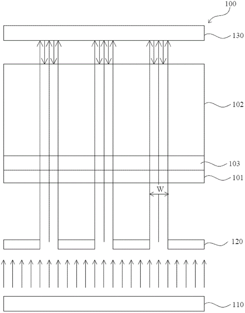
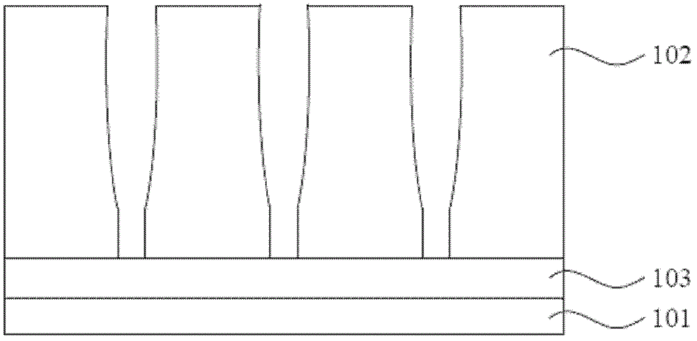
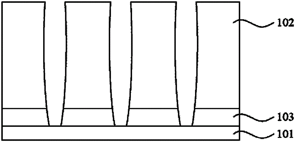
[0028] Please refer to figure 1 , which shows a schematic diagram of an exposure apparatus according to a first embodiment of the present invention. The exposure device 100 of this embodiment is used for exposing the photoresist layer 102 on the transparent substrate 101 to pattern the photoresist layer 102 . Wherein, the transparent substrate 101 is, for examp...


PUM


Abstract

Provided are an exposure device and an exposure method. The exposure method comprises: using an exposure light source (110) to provide light to a photoresist layer (102), the light passing through a photomask (120) and a light transmitting substrate (101) to reach the photoresist layer (102); and using a reflective plate (130) to reflect the light, passing through the light transmitting substrate (101) and the photoresist layer (102), back to the photoresist layer (102). The exposure device and method can reduce the line spacing of a photoresist layer pattern.

Description

【Technical field】 [0001] The invention relates to the field of exposure technology, in particular to an exposure device and an exposure method. 【Background technique】 [0002] Photolithography (photo-lithography) has been widely used in the manufacturing process of various electronic products. Photolithography can be used to expose photoresist (PR) to form different patterns (pattern), but when the pattern of photoresist When the line space is small, the light transmittance is small, resulting in part of the photoresist not being exposed and connected together. Therefore, the pattern formed after photolithography cannot conform to the preset pattern, which greatly limits the electronic Product performance. [0003] In particular, in many current electronic devices, such as liquid crystal display devices, it is necessary to continuously reduce the pitch of patterns to improve the performance of the electronic devices. [0004] Therefore, it is necessary to provide an exposu...

Claims


Application Information

Patent Timeline
Patent Type & Authority Patents(China)
IPC IPC(8): G03F7/20
CPCG03F7/2008
Inventor 施明宏许哲豪薛景峰
Owner TCL CHINA STAR OPTOELECTRONICS TECH CO LTD
Why Eureka
Try Eureka