Preparation method of polycrystal Si films through Ge low-temperature induced crystallization
A low-temperature induction, polycrystalline silicon film technology, applied in ion implantation plating, metal material coating process, coating and other directions, can solve the problems of high substrate requirements, small grain size of polycrystalline Si film, and high crystallization temperature, To achieve the effect of simple process
- Summary
- Abstract
- Description
- Claims
- Application Information
AI Technical Summary
Problems solved by technology
Method used
Image

Examples
Embodiment 1
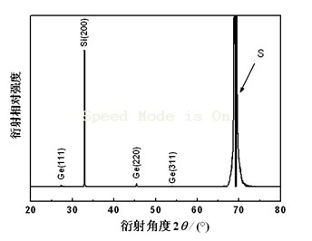
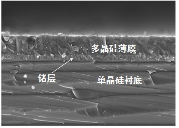
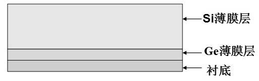
[0028] A preparation method of GE low -temperature induced crystal polycrystalline Si film, which is implemented by the following steps,
[0029] A) 200 ° C grows a 400nm GE landfill layer on the substrate:
[0030] (1) Single crystal Si substrate with a crystal index of 400 passes through acetone ultrasound for 10 minutes, water -free ethanol ultrasound was cleaned for 20 minutes, removed with high -purity nitrogen dried in the magnetic sputtering room with high purity nitrogen;Set the target spacing of the GE target to 80 mm, and the target spacing of the SI target is 60mm;
[0031] (2) The real vacancy of this background is better than 4.0 × 10 -4 After PA, the purity of the passing of 99.999%is high purity;
[0032] (3) By regulating the flow of the gas, the pressure of the growth room work is 2.0Pa, and the substrate temperature is 200 ° C;
[0033] (4) After the substrate temperature and the interior pressure of the studio are stable, the DC power supply of the GE target is ...
Embodiment 2
[0044] A preparation method of GE low -temperature induced crystal polycrystalline Si film, which is implemented by the following steps,
[0045] A) 30 ° C grows a 200nm GE landfill layer on the substrate:
[0046] (1) The substrate with a crystal index of 150 is cleaned by acetone ultrasound for 10 minutes, and the water -free ethanol ultrasound was cleaned for 20 minutes.The target spacing is set to 83 mm, and the target spacing of the SI target is 80mm;
[0047] (2) The real vacancy of this background is better than 4.0 × 10 -4 After PA, the purity of the passing of 99.999%is high purity;
[0048] (3) By regulating the flow of the gas, the pressure of the growth room work is 2.0Pa, and the substrate temperature is 300 ° C;
[0049] (4) After the substrate temperature and the interior pressure of the studio are stable, the DC power supply of the GE target is adjusted to 100 watts, and the GE landment layer is started;
[0050] (5) After 30 minutes of sputtering in the GE target,...
Embodiment 3
[0057] A preparation method of GE low -temperature induced crystal polycrystalline Si film, which is implemented by the following steps,
[0058] A) 500 ° C grows a layer of 500nm GE landfill layer on the substrate:
[0059] (1) Single crystal Si substrate with a crystal index of 500 passes through acetone ultrasound for 10 minutes, water -free ethanol ultrasound was cleaned for 20 minutes, removed with high -purity nitrogen dried in the magnetic sputtering room with high purity nitrogen;Set the target spacing of the GE target to 75 mm, and the target spacing of the SI target is 55mm;
[0060] (2) The real vacancy of this background is better than 4.0 × 10 -4 After PA, the purity of the passing of 99.999%is high purity;
[0061] (3) By regulating the flow of the air, the pressure of the growth room work is 2.0Pa, and the substrate temperature is 500 ° C;
[0062] (4) After the substrate temperature and the interior pressure of the studio are stable, the DC power supply of the GE t...
PUM
| Property | Measurement | Unit |
|---|---|---|
| Thickness | aaaaa | aaaaa |
| Thickness | aaaaa | aaaaa |
Abstract
Description
Claims
Application Information
 - R&D Engineer
- R&D Manager
- IP Professional
- Industry Leading Data Capabilities
- Powerful AI technology
- Patent DNA Extraction
Browse by: Latest US Patents, China's latest patents, Technical Efficacy Thesaurus, Application Domain, Technology Topic.
© 2024 PatSnap. All rights reserved.Legal|Privacy policy|Modern Slavery Act Transparency Statement|Sitemap