
Three-dimensional (3D) display device and manufacture method thereof

A technology of a display device and a manufacturing method, which is applied in the field of 3D display, can solve the problems of increased lens arch height and higher production cost, and achieve the effect of reducing production cost

Active Publication Date: 2012-08-08
BOE TECH GRP CO LTD
View PDF6 Cites 47 Cited by
  • Summary
  • Abstract
  • Description
  • Claims
  • Application Information

AI Technical Summary

Problems solved by technology

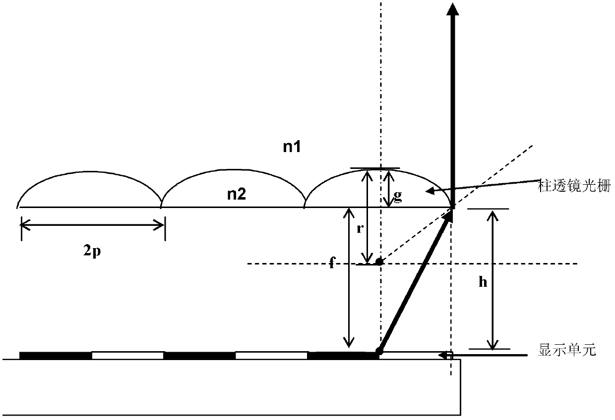
[0009] It can be seen that the existing 3D display device is difficult to solve the problem of high production cost due to the need to additionally manufacture parallax barriers on the display device that has been formed in the box during the process of making the grating layer, or the increase in the arch height of the lens. question

Method used


Image

  • Three-dimensional (3D) display device and manufacture method thereof
  • Three-dimensional (3D) display device and manufacture method thereof
  • Three-dimensional (3D) display device and manufacture method thereof

Examples


Embodiment Construction

[0045] The following will clearly and completely describe the technical solutions in the embodiments of the present invention with reference to the accompanying drawings in the embodiments of the present invention. Obviously, the described embodiments are only some, not all, embodiments of the present invention. Based on the embodiments of the present invention, all other embodiments obtained by persons of ordinary skill in the art without making creative efforts belong to the protection scope of the present invention.

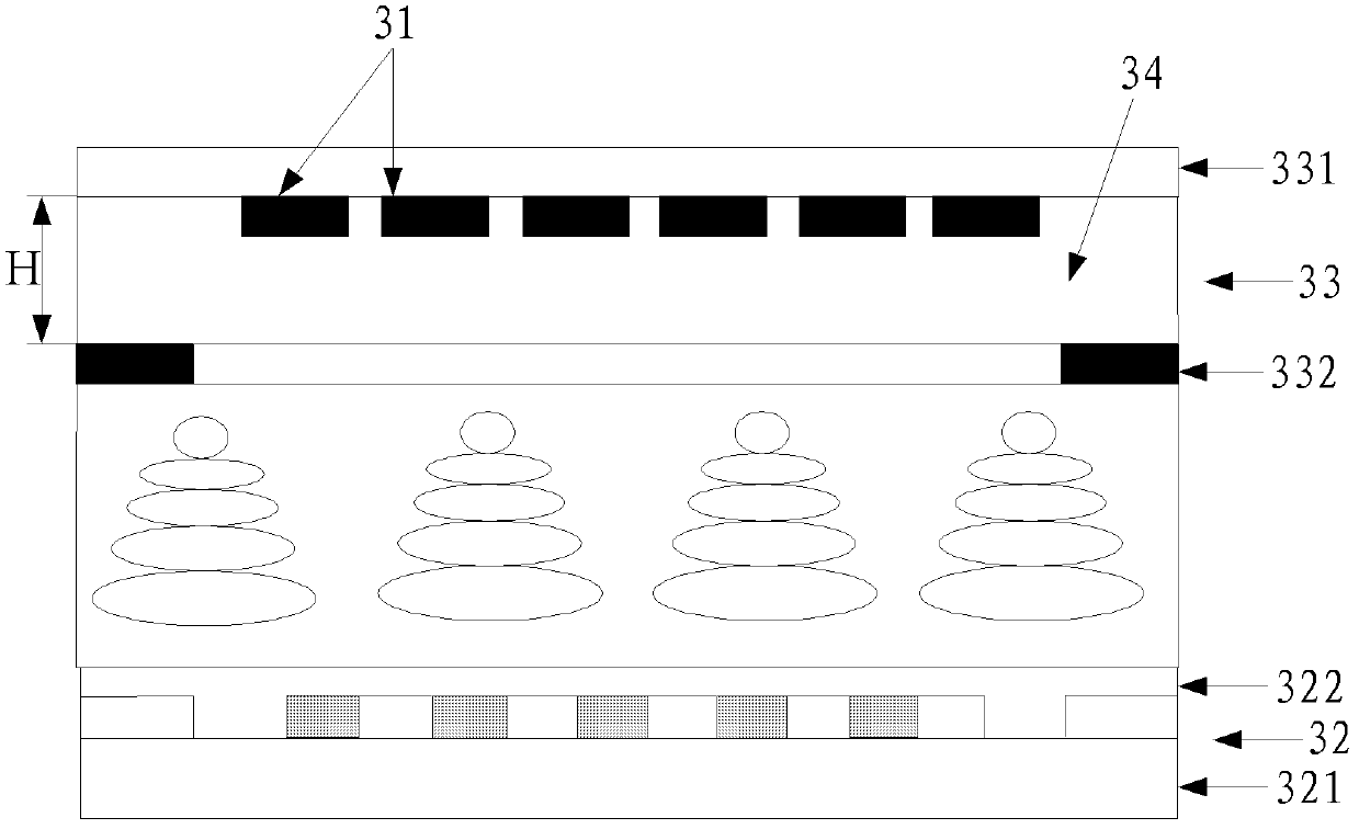
[0046] The 3D liquid crystal display device provided by the embodiment of the present invention, such as image 3 shown, incl.

[0047] The grating layer 31, the TFT array substrate 32 and the color filter substrate 33 formed in the box, wherein the grating layer 31 includes a parallax barrier or lens grating, the color filter substrate 33 includes a transparent substrate 331 and a color filter 332, the TFT array substrate 32 and the color filter Liquid cryst...


PUM

PropertyMeasurementUnit
widthaaaaaaaaaa
thicknessaaaaaaaaaa

Abstract

An embodiment of the invention provides a three-dimensional (3D) display device and a manufacture method thereof, which relate to the technical field of 3D display. A parallax retaining board can be manufactured in a display device box molded through opposite boxes, arch height of a lens is reduced, increasing of new processes or adoption of new production devices is avoided, and production cost is reduced. A 3D liquid crystal display device comprises a grating layer, a thin film transistor (TFT) array substrate molded through opposite boxes and a color film substrate. The TFT array substrate comprises a plurality of pixel units divided through grating lines and data lines crossing transversely and vertically. Each pixel unit comprises a pixel electrode and a TFT circuit. Each pixel electrode of each pixel unit comprises at least two left view field pixel electrodes and at least two right view field pixel electrodes, and the left view field pixel electrodes and the right view field electrodes are at interval. The TFT circuit of each pixel unit comprises a first sub TFT circuit connected with the left view field pixel electrodes and a second sub TFT circuit connected with the right view field pixel electrodes. The embodiment of the 3D display device and the manufacture method are used for manufacturing the 3D display device.

Description

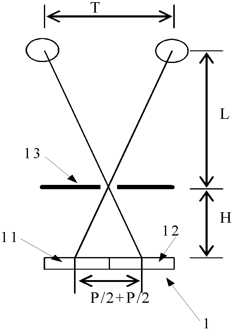
technical field [0001] The present invention relates to the technical field of 3D display, in particular to a 3D display device and a manufacturing method thereof. Background technique [0002] Compared with the 2D display device, the 3D (Three Dimensions, three-dimensional graphics) display device generally needs to install a specific grating layer. At present, there are mainly two methods for realizing the grating layer of the mainstream 3D display device: a parallax barrier method and a lens grating method. [0003] The basic principle of the parallax barrier method is as follows: figure 1 shown. The left-view pixel 11 on the display panel 1 displays a left-eye image, and the right-view pixel 12 displays a right-eye image. A parallax barrier 13 is placed in front of the display panel 1 as a grating layer, and the parallax barrier 13 is composed of alternating light-shielding stripes and light-transmitting stripes. The light-shielding stripes of the parallax barrier 13...

Claims


Application Information

Patent Timeline
Patent Type & Authority Applications(China)
IPC IPC(8): G02F1/1343G02F1/1335G02B27/22G02B5/18H04N13/04G02B30/27G02B30/30
CPCH04N13/04G02F1/1343G02F1/133526G02B27/2214G02F1/133512G02F1/134363G02F2201/124G02F1/13624G02B30/27G02F1/134345G02B30/30H10K59/80515G02B30/00H10K50/00H10K50/813
Inventor 武延兵
Owner BOE TECH GRP CO LTD
Learn More