Light beam array membrane stress measuring device

A technology of array light beams and measuring devices, which is applied in the direction of measuring the force of changes in optical properties of materials when they are stressed, to eliminate stress measurement errors and improve measurement accuracy.

Inactive Publication Date: 2012-08-15
SUZHOU INST OF NANO TECH & NANO BIONICS CHINESE ACEDEMY OF SCI
View PDF8 Cites 6 Cited by
  • Summary
  • Abstract
  • Description
  • Claims
  • Application Information

AI Technical Summary

Problems solved by technology

[0008] The purpose of the present invention is to solve the problem of film stress measurement by the existing laser beam deflection method, and propose an array beam film str

Method used


Image

  • Light beam array membrane stress measuring device
  • Light beam array membrane stress measuring device
  • Light beam array membrane stress measuring device

Examples


Embodiment Construction

[0023] In order to make the array beam thin film stress measurement device of the present invention easier to understand, the technical solution of the present invention will be described in further non-limiting detail below in combination with two preferred embodiments and accompanying drawings.

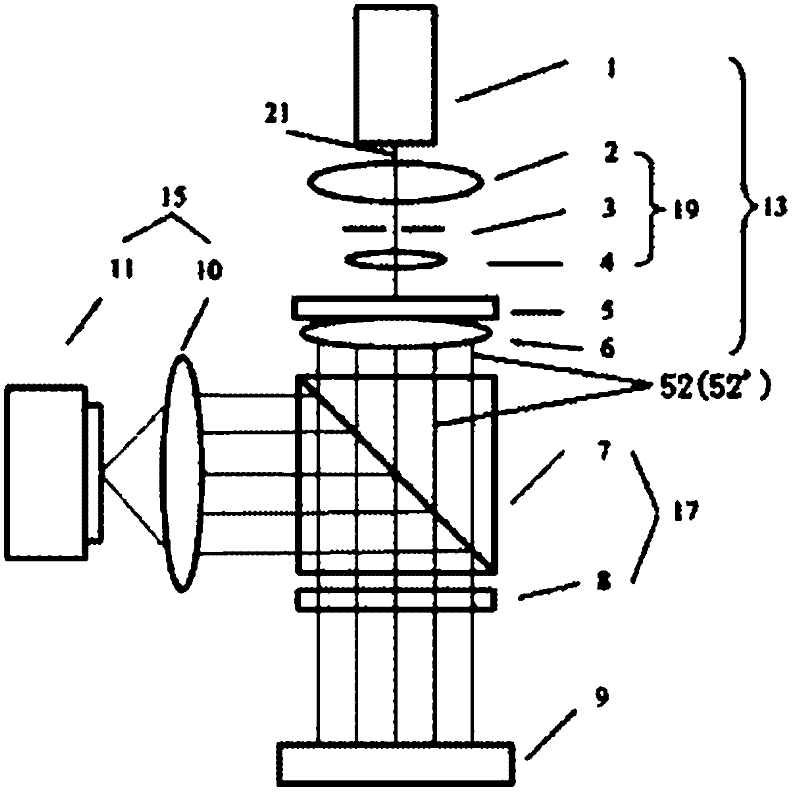
[0024] refer to figure 2 , an array beam film stress measuring device, comprising a multi-beam pattern generator 13, a beam position detector 15 and a beam position separator 17, wherein the multi-beam pattern generator 13 and the beam position detector 15 are arranged perpendicular to each other.

[0025] The multi-beam pattern generator 13 includes a laser 1 , an inverted telescopic collimating optical system 19 , a beam splitter 5 and a collimating lens 6 . Wherein, the inverted telescopic collimation optical system 19 is composed of two lenses 2, 4 and a diaphragm 3 located between the two lenses 2, 4.

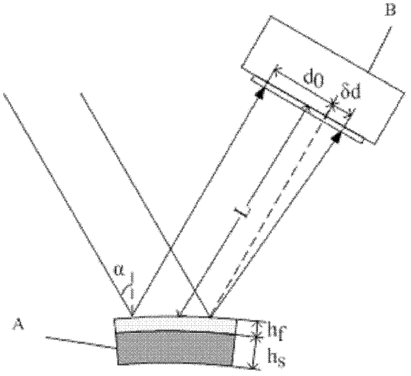
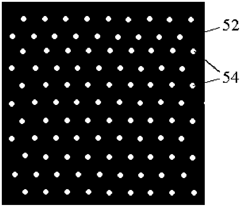
[0026] further reference image 3 and Figure 4 , the above-mentioned b...


PUM


Abstract

The invention discloses a light beam array membrane stress measuring device, which comprises a multi-light-beam pattern generator and a light bema position detector. The multi-light-beam pattern generator comprises a laser device, an inverted telescopic collimation optical system, a beam splitter and a collimation lens. The beam splitter can generate a light beam array, and the light beam array consists of a plurality of mutually parallel single parallel light beams which are arrayed. Accordingly, the light beam array membrane stress measuring device can measure stress distribution of a micro-domain membrane, eliminates stress measurement errors caused by environmental vibration interferences, and improves membrane stress measurement precision.

Description

technical field [0001] The invention relates to a thin film stress measuring device in the field of photoelectric measurement, in particular to an array beam thin film stress measuring device. Background technique [0002] Thin film materials and technologies have been widely used in various fields of high-tech industries such as large-scale integrated circuits, electronic components, flat panel displays, information recording and storage, MEMS, solar cells, optical communications, and semiconductor lighting. In the process of thin film preparation, the mismatch of thermal expansion coefficient and lattice constant between the thin film and the substrate will lead to stress in the grown thin film, and the change of microstructure during the thin film growth process will also cause stress. Excessive film stress will lead to film cracking, curling and even shedding. It can be said that the size of the film stress directly affects the yield, stability, reliability and service ...

Claims


Application Information

Patent Timeline
IPC IPC(8): G01L1/24
Inventor 方运王逸群王玮张永红朱建军张宝顺
Owner SUZHOU INST OF NANO TECH & NANO BIONICS CHINESE ACEDEMY OF SCI
Why Eureka
Try Eureka