Thin film stress measuring device with vertical optical path structure and application thereof
A technology of thin film stress and measuring device, which is applied in the direction of measuring the change force of optical properties when the material is under stress, can solve the problems of the complexity and difficulty of the optical path layout and installation of the instrument, and simplify the optical path layout and installation. Adjusting requirements and improving the effect of measurement accuracy
- Summary
- Abstract
- Description
- Claims
- Application Information
AI Technical Summary
Problems solved by technology
Method used
Image
Examples
Embodiment 1
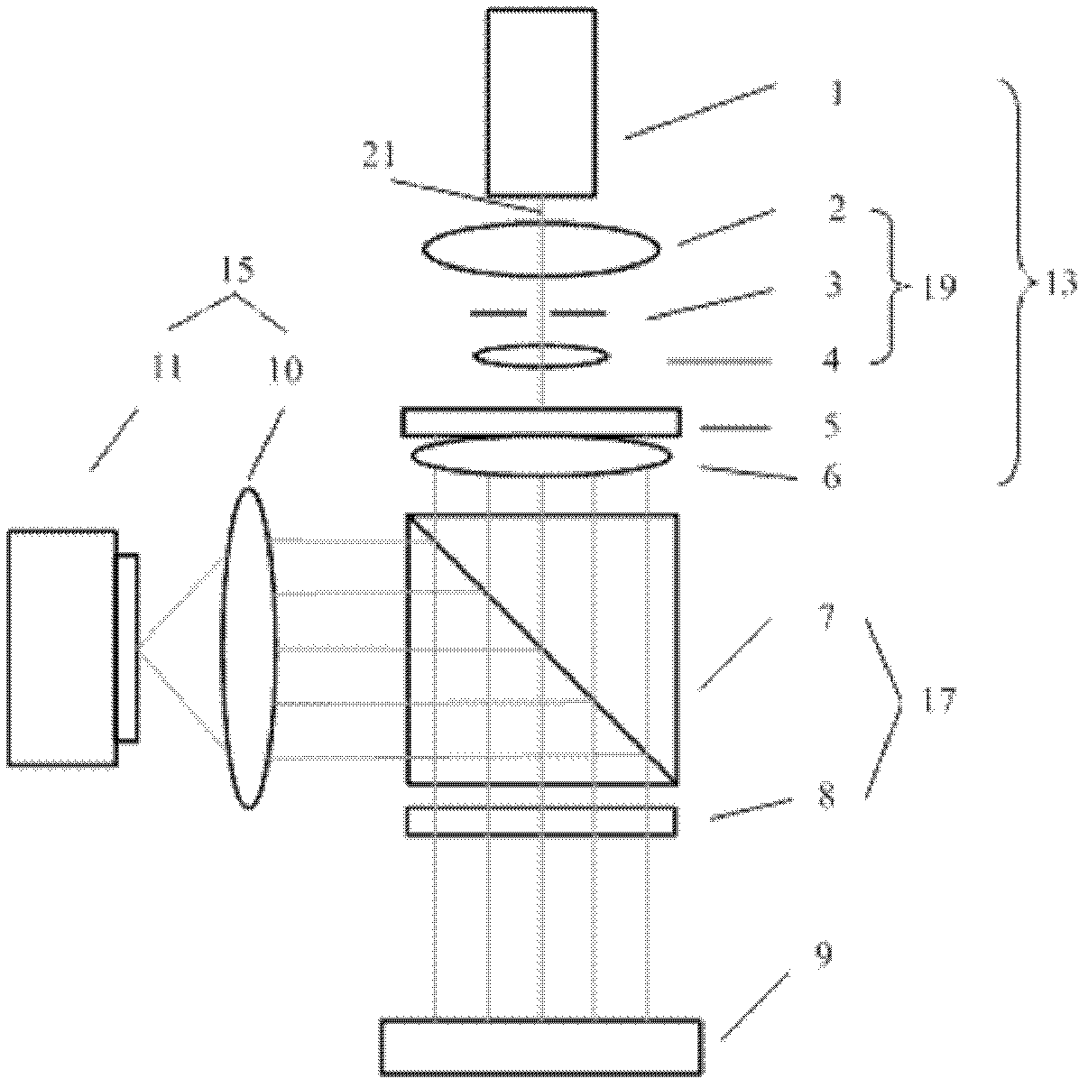
[0024] refer to figure 2 , a film stress measurement device with a vertical optical path structure, including a multi-beam pattern generator 13, a beam position detector 15, and a beam position separator 17, wherein the multi-beam pattern generator 13 and the beam position detector 15 are arranged perpendicularly to each other .
[0025] The multi-beam pattern generator 13 includes a laser 1 , an inverted telescopic collimating optical system 19 , a beam splitter 5 and a collimating lens 6 . Wherein, the inverted telescopic collimation optical system 19 is composed of two lenses 2, 4 and a diaphragm 3 located between the two lenses 2, 4. The beam splitter 5 can be one of a Fabry-Perot etalon, a diffraction grating, a digital micromirror device, a liquid crystal spatial light modulator or a liquid crystal optical phased array device. The single laser beam 21 emitted by the laser 1 is incident on the beam splitter 5 after undergoing beam spot size compression by the inverted ...
Embodiment 2
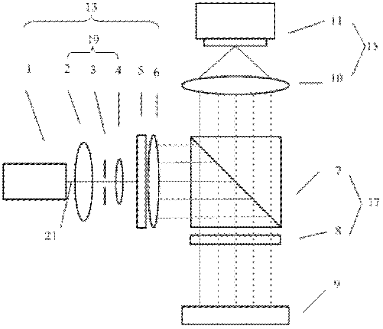
[0034] refer to image 3 Compared with the above-mentioned embodiment 1, the thin-film stress measuring device with vertical optical path structure in embodiment 2 only exchanges the positions of the multi-beam pattern generator 13 and the beam position detector 15, and also arranges them perpendicular to each other. Other components and arrangements have not been changed, so no more details are given here.
[0035] Therefore, the thin film stress measurement device with a vertical optical path structure proposed by the present invention improves the measurement accuracy of the thin film stress by arranging the multi-beam pattern generator and the beam position detector perpendicular to each other, and simplifies the optical path layout of the thin film stress measurement device and adjustment requirements.
PUM
 Abstract
Description
Claims
Application Information


