Electronic devices and systems, and methods for making and using the same

A conductive, nano-scale technology, applied in semiconductor/solid-state device manufacturing, circuits, electrical components, etc., can solve complex problems

Active Publication Date: 2012-08-15
MIE FUJITSU SEMICON
View PDF5 Cites 9 Cited by
  • Summary
  • Abstract
  • Description
  • Claims
  • Application Information

AI Technical Summary

Problems solved by technology

However, both types of devices require more complex and expensive wafers and associated processing than those used in bulk CMOS

Method used


Image

  • Electronic devices and systems, and methods for making and using the same
  • Electronic devices and systems, and methods for making and using the same
  • Electronic devices and systems, and methods for making and using the same

Examples


Embodiment Construction

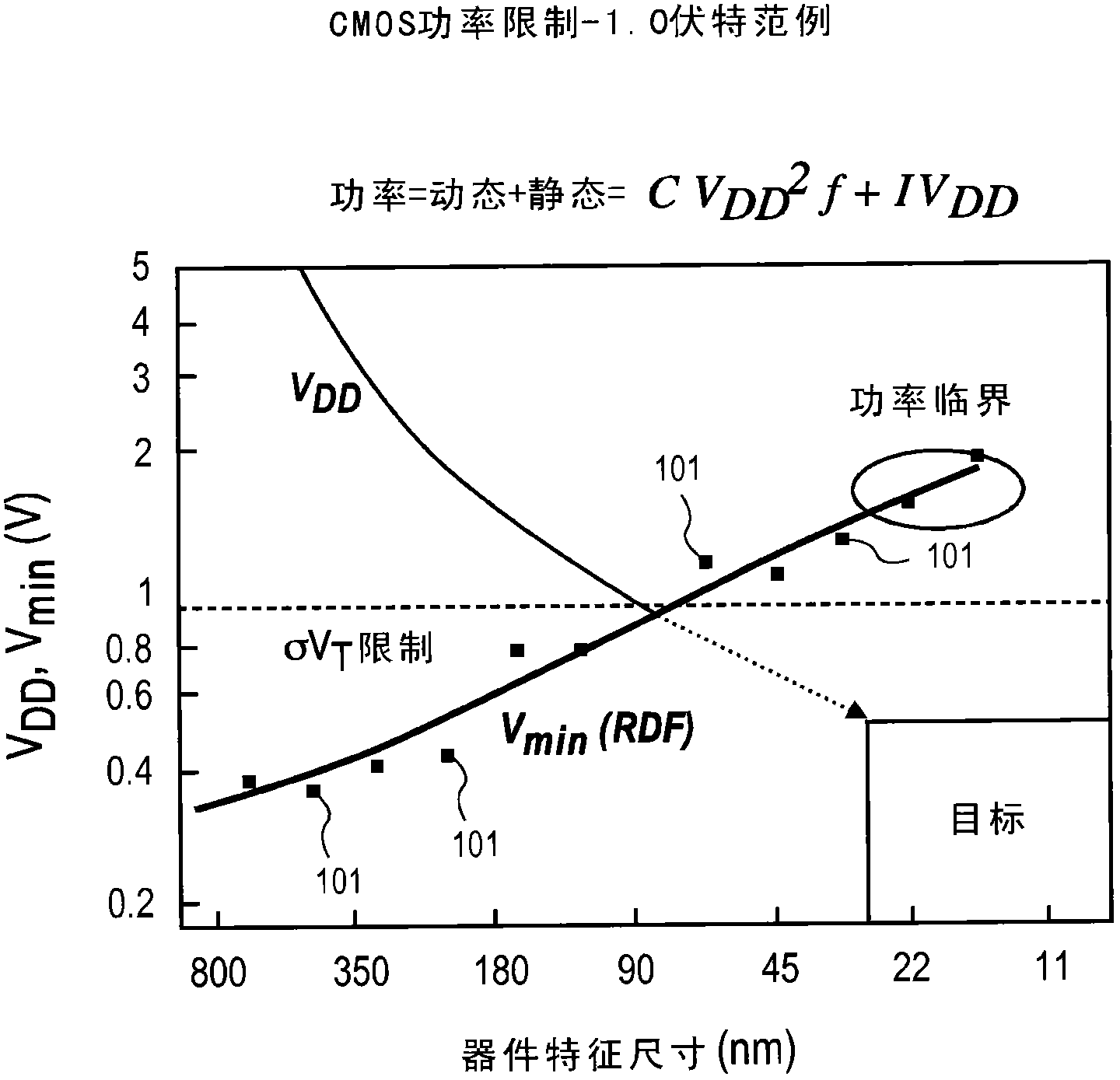
[0085] A novel set of structures and methods are provided to reduce power consumption in large arrays of electronic devices and systems. Some of these structures and methods can be implemented in large numbers by reusing existing bulk CMOS process flows and fabrication techniques, allowing the semiconductor industry, and the electronics industry more broadly, to avoid costly and risky switches to alternative technologies.

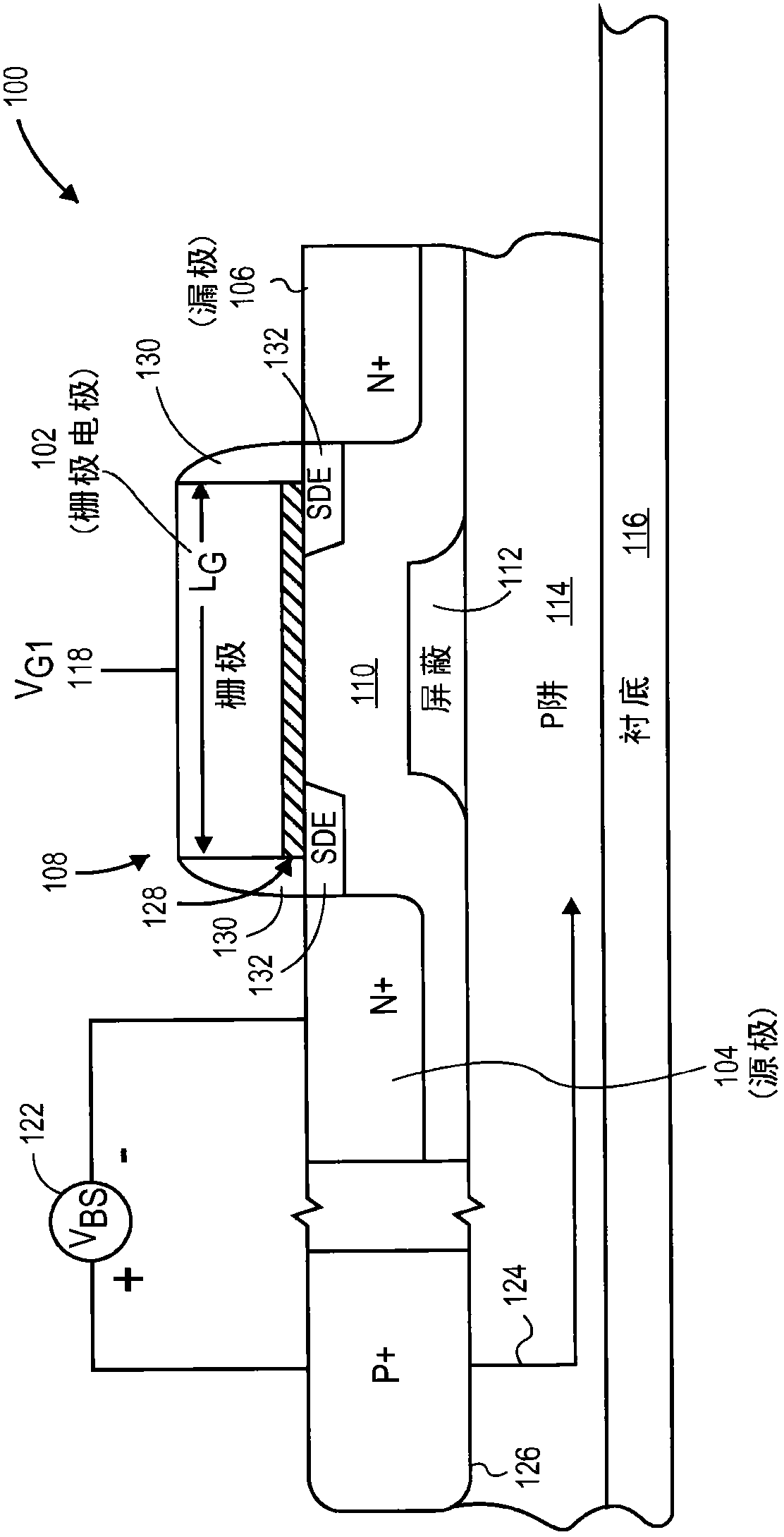
[0086]As noted above, some structures and methods involve deep depletion channel (DDC) designs. DDC can allow CMOS devices with reduced σV compared to traditional bulk CMOS T , and can allow the threshold voltage V of the FET with dopants in the channel region T is set much more precisely. DDC designs can also have a stronger body effect than conventional bulk CMOS transistors, which can allow significant dynamic control of power dissipation in DDC transistors. There are many ways to structure a DDC to achieve different advantages, and the additional fea...


PUM


Abstract

A suite of novel structures and methods is provided to reduce power consumption in a wide array of electronic devices and systems Some structures and methods can be implemented largely by reusing existing bulk CMOS process flows and manufacturing technology, allowing the semiconductor industry as well as the broader electronics industry to avoid a costly and nsky switch to alternative technologies Some structures and methods relate to a Deeply Depleted Channel (DDC) design, allowing CMOS based devices to have a reduced oVT compared to conventional bulk CMOS and can allow the threshold voltage VT ofFETs having dopants in the channel region to be set more precisely The DDC design also can have a strong body effect compared to conventional bulk CMOS transistors, which can allow for significant dynamic control of power consumption in DDC transistors There are many ways to configure the DDC to achieve different benefits.

Description

[0001] related application [0002] This application claims priority to US Provisional Application No. 61 / 247,300, filed September 30, 2009, the contents of which are hereby incorporated by reference in their entirety. This application claims priority to US Provisional Application No. 61 / 262,122, filed November 17, 2009, the contents of which are hereby incorporated by reference in their entirety. This application claims priority to US Provisional Application No. 12 / 708,497, filed February 18, 2010, the contents of which are hereby incorporated by reference in their entirety. Background technique [0003] Electronic devices have become a part of everyday life more than ever before. Systems such as personal computers and mobile phones have fundamentally changed how we work, play and communicate. Every year new devices are introduced, such as digital music players, e-book (electronic book) readers and tablet computers, as well as improvements to existing product families. Th...

Claims


Application Information

Patent Timeline
Patent Type & Authority Applications(China)
IPC IPC(8): H01L21/335H10B10/00
CPCH01L21/823412H01L21/823493H01L21/84H01L27/0207H01L29/105H01L29/1079H01L29/66545H01L29/66628H01L29/7834H10B10/00H10B10/12
Inventor 斯科特·E·汤普森达莫代尔·R·图马拉帕利
Owner MIE FUJITSU SEMICON
Why Eureka
Try Eureka