
Imaging device and camera module

A technology for imaging devices and camera modules, which can be applied to electric solid-state devices, semiconductor devices, electrical components, etc., can solve problems such as thermal deformation of chips, and achieve the effect of suppressing flash.

Active Publication Date: 2012-08-29
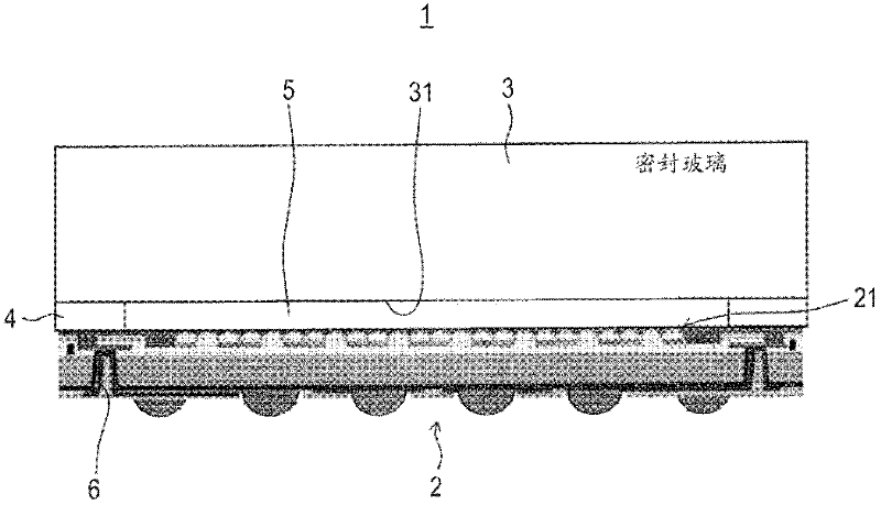
SONY CORP
View PDF6 Cites 3 Cited by
  • Summary
  • Abstract
  • Description
  • Claims
  • Application Information

AI Technical Summary

Problems solved by technology

[0008] However, when a through hole (TSV) is formed in the CSP structure, the chip is formed thin in thickness, and therefore, there is a danger that when there is a gap 5 between the cover glass and the chip (optical chip) as described above, Thermal deformation of the chip due to thermal stress during heat treatment such as reflow

Method used


Image

  • Imaging device and camera module
  • Imaging device and camera module
  • Imaging device and camera module

Examples


Embodiment Construction

[0038] Embodiments of the present disclosure are described below with reference to the drawings.

[0039] Description will be given in the following order.

[0040] 1. First structure example of imaging device

[0041] 2. Control the basic structure and function of the film (multilayer film)

[0042] 3. Control the specific structure and function of the film (multilayer film)

[0043] 4. Typical structure and function of control film (multilayer film)

[0044] 5. Second structure example of imaging device

[0045] 6. Structure example of camera module

[0046]

[0047] Figure 5 is a view showing a first structural example of the imaging device according to the embodiment.

[0048] In this embodiment, a CMOS image sensor (CIS) is used as an example of an optical sensor.

[0049] The imaging device 100 according to this embodiment mainly has a CSP structure in which the chip size of the optical sensor is packaged, and a cavity-less CPS structure without gaps in which t...


PUM


Abstract

An imaging device includes: an optical sensor including a light receiving unit capable of forming an object image; a seal material for protecting the light receiving unit of the optical sensor; an intermediate layer formed at least between the light receiving unit and an opposite surface of the seal material facing the light receiving unit; and a control film arranged between the intermediate layer and the opposite surface of the seal material, wherein, in the control film, a cutoff wavelength is shifted to a shortwave side in accordance with an incident angle of light which is obliquely incident on the film.

Description

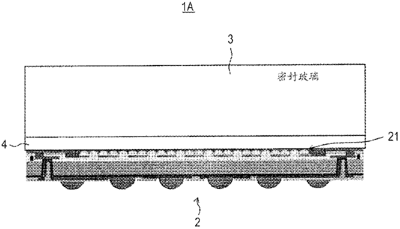
technical field [0001] The present disclosure relates to an imaging device and a camera module including an optical sensor such as a CCD image sensor or a CMOS image sensor (CIS) as a chip scale package. Background technique [0002] As a simple packaging method for optical sensors, a chip scale package (CSP) structure has been proposed. [0003] figure 1 is a view showing the basic structure of the CSP structure. [0004] In the CSP structure 1 of FIG. 1 , a sealing glass (cover glass) 3 is disposed on the front surface of the optical sensor (sensor chip) 2 as a sealing member for protecting the upper portion of the light receiving unit 21 . [0005] In the CSP structure 1 , excluding the light receiving unit 21 of the optical sensor 2 , the sealing glass 3 is disposed through the resin 4 arranged in the peripheral portion. Therefore, in the CSP structure, a gap 5 is formed between the light receiving unit 21 of the optical sensor 2 and the opposing surface 31 of the sea...

Claims


Application Information

Patent Timeline
Patent Type & Authority Applications(China)
IPC IPC(8): H01L27/146H04N5/225H04N5/335H04N25/00
CPCH01L27/14618H01L27/14621H01L27/14625H01L2224/13H01L2224/48091H01L2224/73265H01L2924/00014H01L27/148H01L27/146
Inventor 汤川弘章前田兼作高地泰三丸山康
Owner SONY CORP
Learn More