Method of manufacturing solid-state imaging element, solid-state imaging element and electronic apparatus

A technology of solid-state imaging components and manufacturing methods, which can be applied to electric solid-state devices, radiation control devices, electrical components, etc., and can solve problems such as chip cracks

Inactive Publication Date: 2012-08-29
SONY SEMICON SOLUTIONS CORP
View PDF9 Cites 22 Cited by
  • Summary
  • Abstract
  • Description
  • Claims
  • Application Information

AI Technical Summary

Problems solved by technology

Therefore, in these methods, since stress is applied to the outer periphery of a chip having a...

Method used


Image

  • Method of manufacturing solid-state imaging element, solid-state imaging element and electronic apparatus
  • Method of manufacturing solid-state imaging element, solid-state imaging element and electronic apparatus
  • Method of manufacturing solid-state imaging element, solid-state imaging element and electronic apparatus

Examples


Embodiment 1-2

[0084] 3. Embodiment 1-2 (an example of bending an imaging chip by gas volume contraction)

Embodiment 1-3

[0085] 4. Embodiments 1-3 (example using a base as a package)

[0086] 5. Embodiments 1-4 (Example of fixing the imaging chip to the base by vacuum adsorption)

[0087] 6. Example 2-1 (example of bending an imaging chip by curing shrinkage of resin)

Embodiment 2-2

[0088] 7. Embodiment 2-2 (example of bending the imaging chip by negative pressure)

[0089] 8. Embodiment 2-3 (Example using a base as a package)

[0090] 9. Embodiment 2-4 (Example of fixing the imaging chip to the base by vacuum adsorption)

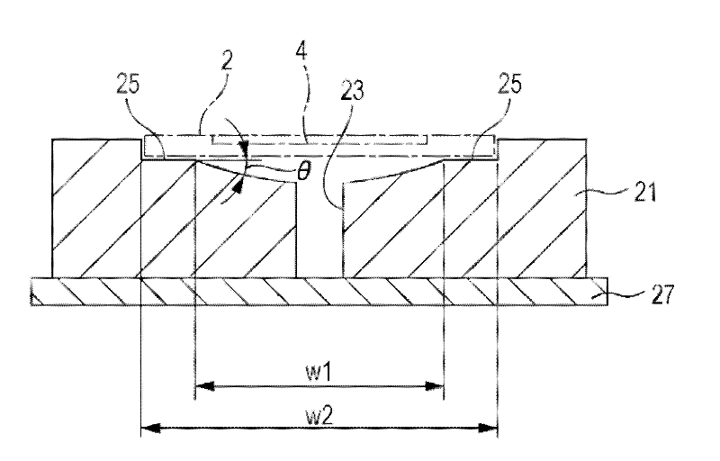
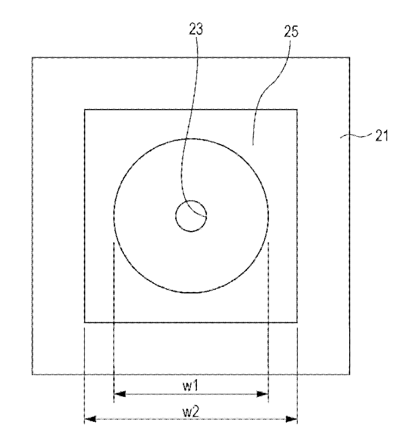
[0091] 10. Embodiment 2-5 (example of controlling the shape of the curved part according to the shape of the base)

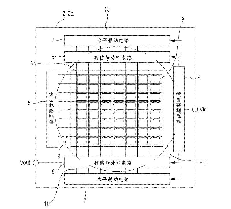
[0092] 11. Schematic structural example of a solid-state imaging chip applied to the present invention


PUM


Abstract

A method of manufacturing a solid-state imaging element includes: manufacturing an element chip in which photoelectric conversion units are arranged on a main surface side; preparing a base configured using a material with an expansion coefficient greater than the element chip and having an opening of which the periphery of the opening is shaped as a flat surface; expanding the base by heating, mounting the element chip on the flat surface of the base in a state where the opening of the base is covered; and three-dimensionally curving a portion corresponding to the opening in the element chip by cooling and contracting the base in a state where the element chip is fixed to the flat surface of the expanded base.

Description

[0001] Cross References to Related Applications [0002] This application contains the Japanese priority patent application JP 2011-043015 submitted to the Japan Patent Office on February 28, 2011, the Japanese priority patent application 2011-042447 submitted to the Japan Patent Office on February 28, 2011, and the Japanese priority patent application JP 2011 on February 28, 2011 The disclosure of Japanese Priority Patent Application JP 2011-043014 filed in the Japan Patent Office in Japan is hereby incorporated by reference in its entirety. technical field [0003] The present invention relates to a manufacturing method for manufacturing a solid-state imaging element in which photoelectric conversion units are arranged on a three-dimensionally curved curved surface, a solid-state imaging element obtained by the manufacturing method, and an electronic device provided with the solid-state imaging element. [0004] Furthermore, the present invention also relates to a solid-stat...

Claims


Application Information

Patent Timeline
IPC IPC(8): H01L27/146
CPCH01L27/14618H01L31/0203H01L2924/0002H01L2924/00H01L27/146
Inventor 糸长总一郎
Owner SONY SEMICON SOLUTIONS CORP
Why Eureka
Try Eureka