Surface modified nano-abrasive silicon slice polishing liquid
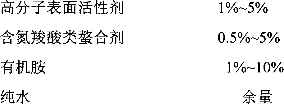
A surface modification technology for nanometer and silicon wafer polishing, which is applied in the direction of polishing compositions containing abrasives, etc., can solve the problems of silicon wafer surface damage, complicated cleaning steps, and difficult cleaning, etc., to reduce roughness and improve microscopic conditions Effect
- Summary
- Abstract
- Description
- Claims
- Application Information
AI Technical Summary
Problems solved by technology
Method used
Image
Examples
Embodiment 1
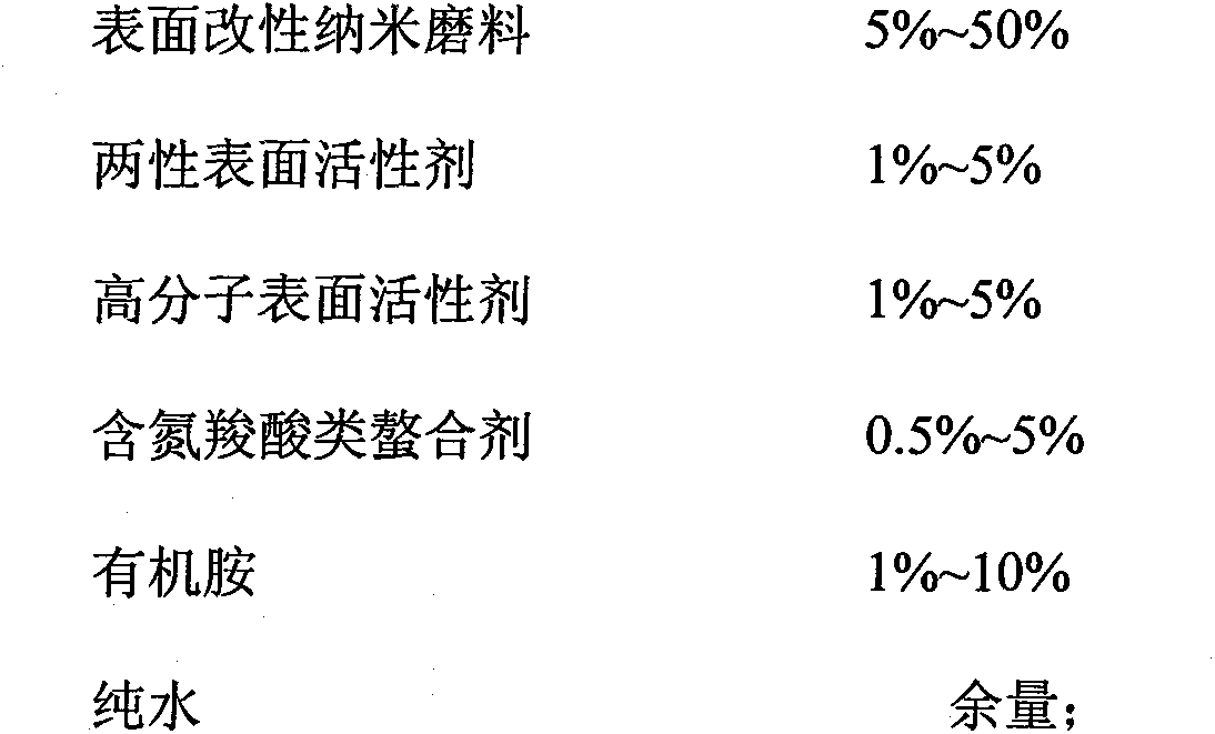
[0021] Example 1: Polystyrene SiO 2 Modified nano-abrasive 5%;
[0022] Sodium laurylalanine 2%;
[0023] Macrogol 400 2%;
[0024] EDTA 1%;
[0025] Tetramethylammonium hydroxide 1%;
[0026] The balance of pure water, the pH value of the solution is 11.5.
[0027] Prepare the polishing liquid according to the above-mentioned specific implementation method and carry out the polishing experiment. After polishing, the material removal rate is R=780nm, and the surface roughness R a = 0.10 nm.
Embodiment 2
[0028] Example 2: Polystyrene SiO 2 Modified nano-abrasive 20%;
[0029] Sodium laurylalanine 1%;
[0030] Macrogol 400 2%;
[0031] EDTA 1%;
[0032] Tetramethylammonium hydroxide 1%;
[0033] The balance of pure water, the pH value of the solution is 11.2.
[0034] Prepare polishing liquid according to above-mentioned specific implementation method and carry out polishing experiment, the material removal rate after polishing is R=820nm, surface roughness R a = 0.10 nm.
Embodiment 3
[0035] Example 3: Polystyrene SiO 2 Modified nano-abrasive 20%;
[0036] Sodium Octadecylalanine 3%;
[0037] Macrogol 400 2%;
[0038] EDTA disodium salt 1%;
[0039] Tetraethylammonium hydroxide 1%;
[0040] The balance of pure water, the pH value of the solution is 11.4.
[0041] Prepare polishing liquid according to above-mentioned specific implementation method and carry out polishing experiment, the material removal rate after polishing is R=820nm, surface roughness R a = 0.10 nm.
PUM
| Property | Measurement | Unit |
|---|---|---|
| particle diameter | aaaaa | aaaaa |
| electrical resistance | aaaaa | aaaaa |
| surface roughness | aaaaa | aaaaa |
Abstract
Description
Claims
Application Information


