
Lens array and optical module provided therewith

一种透镜阵列、透镜面的技术,应用在光学、光学元件、光导等方向,能够解决制造困难等问题

Inactive Publication Date: 2012-09-12
ENPLAS CORP
View PDF23 Cites 59 Cited by
  • Summary
  • Abstract
  • Description
  • Claims
  • Application Information

AI Technical Summary

Problems solved by technology

Therefore, when the structure described in Patent Document 1 is applied to a lens array, there is a problem that it is difficult to form a reflection surface for reflecting monitor light around the lens.
[0013] In addition, in Patent Document 2, since the positional accuracy of the boundary between the total reflection mirror and the notch is required, there is a problem that manufacturing is difficult.

Method used


Image

  • Lens array and optical module provided therewith
  • Lens array and optical module provided therewith
  • Lens array and optical module provided therewith

Examples


Embodiment approach 1

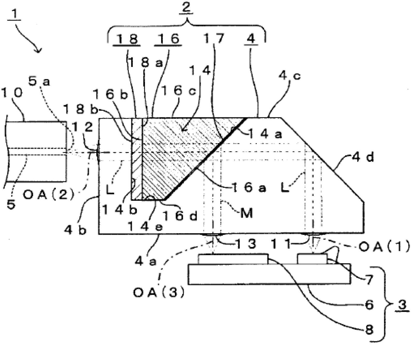
[0089] Below, refer to Figure 1 to Figure 6 Embodiment 1 of the lens array of the present invention and an optical module including the lens array will be described.

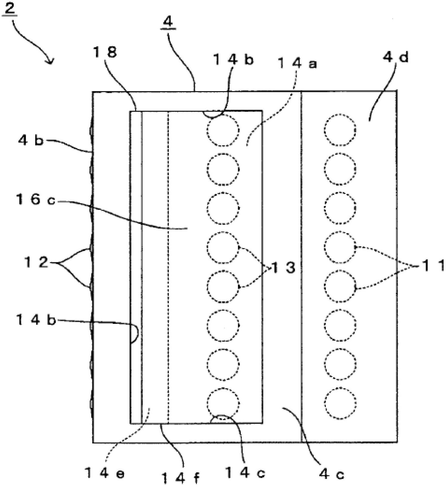
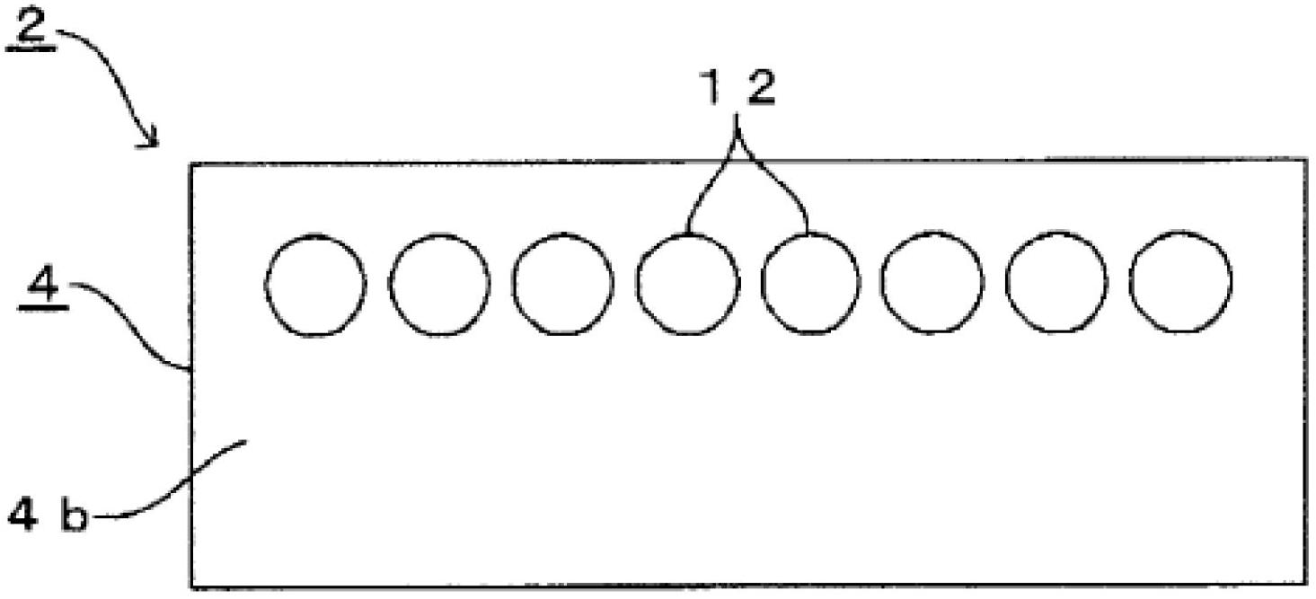
[0090] figure 1 It is the outline of the optical module 1 in this embodiment and the longitudinal cross-section of the lens array 2 in this embodiment. Figure 1 The schematic structure diagram shown. figure 2 yes figure 1 A top view of the lens array 2 shown. image 3 yes figure 1 Left side view of lens array 2 is shown. Figure 4 yes figure 1 Right side view of lens array 2 shown. Figure 5 yes figure 1 Bottom view of lens array 2 shown.

[0091] Such as figure 1 As shown, the lens array 2 in this embodiment is arranged between the photoelectric conversion device 3 and the optical fiber 5 .

[0092] Here, the photoelectric conversion device 3 has a plurality of light emitting elements 7 on the surface of the semiconductor substrate 6 facing the lens array 2, and the plurality of light emitti...

Embodiment approach 2

[0139] Next, regarding Embodiment 2 of the lens array of the present invention and an optical module including the same, focusing on the differences from Embodiment 1, refer to Figure 7 ~ Figure 12 Be explained.

[0140] In addition, in this embodiment, for the Figure 1 to Figure 6 For parts with the same or similar structure, use the same Figure 1 to Figure 6 The same reference numerals are used for description.

[0141] Figure 7 It is the outline of the optical module 21 in this embodiment and the longitudinal cross-section of the lens array 22 in this embodiment. Figure 1 The schematic structure diagram shown. Figure 8 yes Figure 7 A top view of lens array 22 is shown. Figure 9 yes Figure 8 Left side view of the lens array shown. Figure 10 yes Figure 8 Right side view of the lens array shown. Figure 11 yes Figure 8 Bottom view of the lens array shown.

[0142] In this embodiment, as one of the differences from Embodiment 1, when fixing the photoelec...

Embodiment approach 3

[0153] Hereinafter, regarding Embodiment 3 of the lens array of the present invention and an optical module including the same, focusing on differences from Embodiments 1 and 2, refer to Figure 13 to Figure 16 Be explained.

[0154] In addition, in this embodiment, for the Figure 1 to Figure 12 For parts with the same or similar structure, use the same Figure 1 to Figure 12 The same reference numerals are used for description.

[0155] Figure 13 It is the outline of the optical module 30 in this embodiment and the longitudinal section of the lens array 31 in this embodiment. Figure 1 The schematic structure diagram shown. Figure 14 yes Figure 13 A top view of lens array 31 is shown. Figure 15 yes Figure 14 Right side view of lens array 31 is shown.

[0156] Such as Figure 13 As shown, in this embodiment, the structure is similar to that of Embodiment 2 in that the side surface of the concave portion 14 extends upward from the first optical surface 14a and th...


PUM


Abstract

Provided is a lens array that can reliably obtain monitor light and is easy to manufacture. In the provided lens array, light incident on a first lens surface (11) from light-emitting elements is split by a reflective / transmissive layer (17) between a first optical surface (14a) and a first prism surface (16a) and sent, respectively, towards a second lens surface (12) and a third lens surface (13). Monitor light included in the light sent towards the third lens surface (13) is sent by the third lens surface (13) towards a light-receiving element (8). The path of light incident on the first optical surface (14a) is collinear with the path of light outgoing from the second optical surface (14b).

Description

technical field [0001] The present invention relates to a lens array and an optical module provided with the lens array, and particularly relates to a lens array suitable for optically coupling a plurality of light emitting elements with an end face of a light transmission body and an optical module provided with the lens array. Background technique [0002] In recent years, so-called optical interconnection (optical interconnection) has been widely used as a technology for high-speed signal transmission within a system device, between devices, or between optical modules. Here, the term "optical interconnection" refers to a technique in which optical components are treated as electronic components and mounted on motherboards or circuit boards used in computers, vehicles, optical transceiver modules, and the like. [0003] Optical modules for such optical interconnects, e.g., in-device or in-device with media converters or interconnections of switching hubs, optical transceiv...

Claims


Application Information

Patent Timeline
Patent Type & Authority Applications(China)
IPC IPC(8): G02B6/42
CPCG02B6/4214G02B6/4286G02B6/425G02B6/4292G02B6/4206G02B6/4246
Inventor 森冈心平
Owner ENPLAS CORP
Learn More