Circuit member, manufacturing method of the circuit member, and semiconductor device including the circuit member

a manufacturing method and circuit technology, applied in semiconductor devices, semiconductor/solid-state device details, electrical apparatus, etc., can solve the problems of cracking sealing resin, high possibility of serious damage to the life of society, and adhesion strength (or joining strength) between metals, so as to enhance the reliability of semiconductor devices, and improve the reliability

Inactive Publication Date: 2009-06-11
DAI NIPPON PRINTING CO LTD
View PDF8 Cites 35 Cited by
  • Summary
  • Abstract
  • Description
  • Claims
  • Application Information

AI Technical Summary

Benefits of technology

[0012]The present invention was made in view of challenges as described above, and therefore it is an object to provide the circuit member which can enhance the reliability of the semiconductor device that is finally obtained. It is another object of the present invention to provide the manufacturing method for producing the circuit member which can enhance the reliability of the semiconductor device. It is still another object of the present invention to provide the semiconductor device having significantly higher reliability.
[0013]With intensive studies for achieving the above objects, we have found that the reliability of the semiconductor device that is finally obtained can be significantly enhanced by forming a predetermined roughened face or faces on a surface of the lead frame material of the circuit member as well as by forming a plated layer or layers on the surface of the lead frame material. More specifically, we have found that the adhesiveness between the circuit member and the sealing resin can be markedly enhanced by forming the roughened face or faces having a predetermined surface roughness on the surface of the lead frame material. Besides, we have found that the adhesiveness between the lead part and the bonding wire that can be used for the electrical connection relative to the semiconductor chip and / or adhesiveness between the lead part and soldering portion that can be used for the electrical connection relative to the implementing substrate (or printed circuit board) can be highly improved by laminating a plated layer, such as a Ni plated layer (this term will also be used below as one meaning a nickel plated layer), a Pd plated layer (this term will also be used below as one meaning a palladium plated layer), an Au plated layer (this term will also be used below as one meaning a gold plated layer), and / or an Ag plated layer (this term will also be used below as one meaning a silver plated layer), on the surface of the lead frame material (lead frame body, lead frame member). The present invention is based on such knowledge and / or discovery, and is intended to enhance the reliability of the semiconductor device, by improving the adhesiveness between the circuit member and the sealing resin as well as by enhancing the adhesiveness between the circuit member and the bonding wire and / or soldering portion.

Problems solved by technology

Thus, a fault of the semiconductor device might have a higher possibility to cause a serious damage to the life in society.
In this case, there is a problem of adhesion strength (or joining strength) between the metal and the resin in such an interface region.
If the adhesion strength between the die pad and lead part of the lead frame and the sealing resin is substantially low, peeling between the die pad and lead part of the lead frame and the sealing resin may tend to occur, thus causing a crack in the sealing resin due to such peeling, and even bringing the semiconductor device into a fault, during a manufacturing process of the semiconductor device, during a process of assembling the semiconductor device onto an implementing substrate (or printed circuit board) that will be further mounted onto the electric equipment, and / or during use of such electronic equipment.
That is to say, due to lack or insufficiency of the adhesion strength between the die pad and lead part of the lead frame relative to the sealing resin, the reliability of the semiconductor device will be deteriorated.
In this case, however, no measure is taken for the lead part of the lead frame.
Accordingly, the adhesion strength at the interface between the lead part and the sealing resin cannot be enhanced.
Therefore, the reliability of the semiconductor device cannot be sufficiently improved.
However, in the case of using the organic-acid type etching liquid for the rolled copper plate or rolled copper-alloy plate, such as the lead frame material, it will be impossible or quite difficult to form a surface profile including finely pointed needle-like projections.
Accordingly, it will also be impossible to sufficiently enhance the adhesion strength between the lead frame formed from the rolled copper plate or rolled copper-alloy plate and the sealing resin.

Method used


Image

  • Circuit member, manufacturing method of the circuit member, and semiconductor device including the circuit member
  • Circuit member, manufacturing method of the circuit member, and semiconductor device including the circuit member
  • Circuit member, manufacturing method of the circuit member, and semiconductor device including the circuit member

Examples


first embodiment

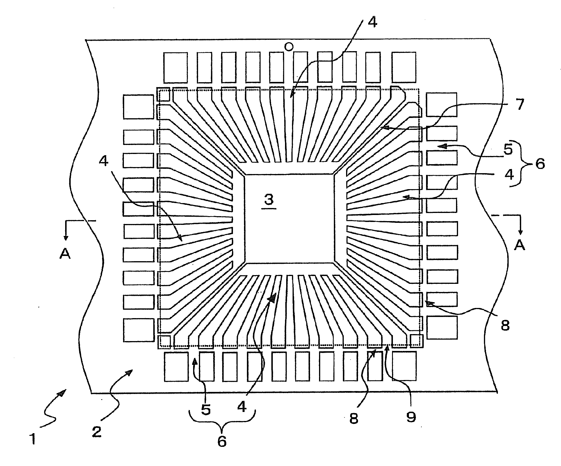
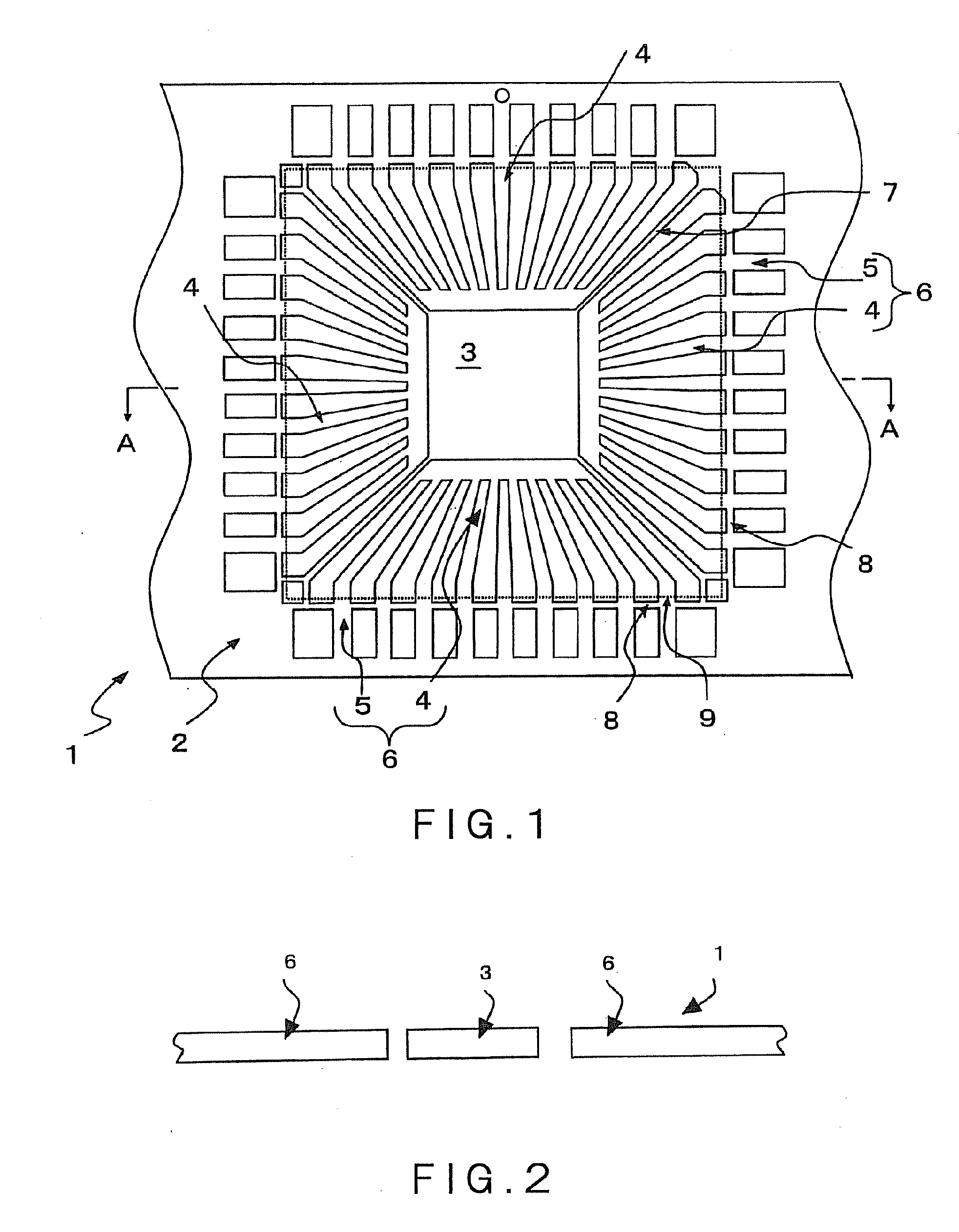
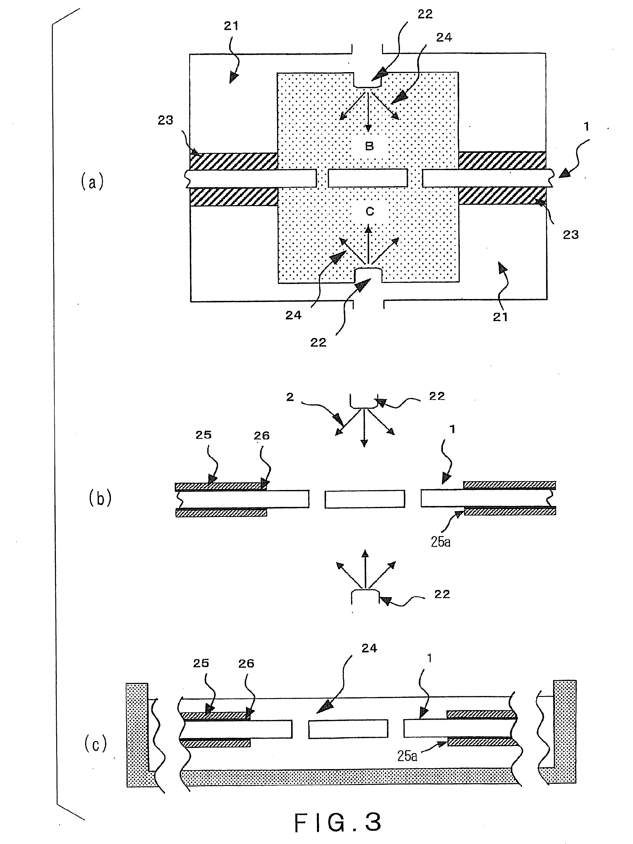
[0060]First of all, a first embodiment of the present invention will be described with reference to FIGS. 1 to 8. Of these drawings, FIG. 1 is a top view of the lead frame material of the QEP type, and FIGS. 2 to 8 are provided for illustrating the circuit member, a manufacturing method for the circuit member and a semiconductor device including the circuit member, respectively seen from a viewpoint corresponding to a cross section taken along line A-A of FIG. 1.

(Construction of the Circuit Member)

[0061]The lead frame material (lead frame body, lead frame member) 1 related to this embodiment is manufactured from a rolled copper plate or rolled copper alloy plate having an elongated plate-like or coil-like shape. In more detail, the lead frame material 1 is formed, in succession, in the rolled copper plate or rolled copper-alloy plate, by etching employing photolithography technology or punching with a press using a mold (mold tool, die), or the like means. That is to say, a pluralit...

second embodiment

[0092]Next a second embodiment according to the present invention will be described with reference to FIGS. 9 to 15. FIGS. 9 to 15 are provided for illustrating the circuit member, the manufacturing method for the circuit member and the semiconductor device including the circuit member, respectively related to the second embodiment and seen from a viewpoint corresponding to the cross section taken along line A-A of FIG. 1. It is noted that in the second embodiment shown in FIGS. 9 to 15, like parts in the first embodiment will be designated by like reference numerals, and repeated description thereof will be omitted below.

(Construction of the Circuit Member)

[0093]As shown in FIG. 9, the lead frame material (lead frame body, lead frame member) 1 related to the second embodiment has substantially the same construction as that of the first embodiment shown in FIG. 1. Therefore, the description about the lead frame material 1 of the second embodiment will now be omitted.

[0094]As shown i...


PUM

PropertyMeasurementUnit
roughnessaaaaaaaaaa
thicknessaaaaaaaaaa
roughness Raaaaaaaaaaa

Abstract

A circuit member 20 includes a lead frame material 1 having a die pad 3, a lead part 6 to be electrically connected with a semiconductor chip 30, and an outer frame 2 configured to support the die pad and the lead part. The lead frame material includes a resin sealing region 9. Roughened faces 10A to 10C and 11A to 11C, each having an average roughness Ra of 0.3 μm or greater, are formed on a surface in the resin sealing region of the lead frame material. The surface of the lead frame material except for the resin sealing region is a flat and smooth face. A two-layer plated layer 12A formed by laminating a Ni plated layer 13 and a Pd plated layer 14 in this order or a three-layer plated layer 12B formed by laminating the Ni plated layer 13, the Pd plated layer 14 and an Au plated layer 15 in this order is formed on the whole surface of the lead frame material.

Description

TECHNICAL FIELD[0001]The present invention relates to a circuit member configured to be electrically connected with a semiconductor chip so as to constitute a part of a semiconductor device, and in particular relates to the circuit member which can enhance reliability of the semiconductor device that is finally obtained. In addition, the present invention relates to a manufacturing method by which such a circuit member can be produced. Furthermore, such the present invention relates to the semiconductor device including the circuit member and exhibiting higher reliability.BACKGROUND ART[0002]In recent years, the semiconductor device has been made to exhibit a higher function and have a more highly integrated structure, and has been mounted on a variety of electronic equipment. Additionally, the semiconductor device has brought greater facility to the life in society and become necessary and essential for the life in society. Thus, a fault of the semiconductor device might have a hig...

Claims


Application Information

Patent Timeline
Patent Type & Authority Applications(United States)
IPC IPC(8): H01L23/495C23F1/00
CPCC25D5/12H01L23/3142H01L2924/01033H01L2924/01006H01L2924/00014H01L2924/014H01L2924/01088H01L2924/01082H01L2924/01079H01L2924/01078H01L2924/01047H01L2924/01046H01L2924/01029H01L2924/01028H01L2924/01027H01L2924/01005H01L2224/92247H01L2224/92H01L2224/85464H01L2224/85385H01L23/49548H01L23/49582H01L24/32H01L24/45H01L24/48H01L24/85H01L2224/32057H01L2224/32245H01L2224/45144H01L2224/48091H01L2224/48247H01L2224/484H01L2224/48599H01L2224/73265H01L2224/83385H01L2224/78H01L2924/3512H01L2924/00H01L2924/00012H01L24/73H01L2224/45015H01L2224/48664H01L2924/181H01L2924/18301
Inventor SHIMAZAKI, YOSAITO, HIROYUKIMASUDA, MASACHIKAMATSUMURA, KENJIFUKUCHI, MASARUIKEZAWA, TAKAO
Owner DAI NIPPON PRINTING CO LTD
Why Eureka
Try Eureka