

Plasma processing apparatus and plasma processing method
一种等离子体、处理装置的技术,应用在真空容器内进行清洁领域,达到抑制损伤、溅射作用降低、高电子密度的效果
Inactive Publication Date: 2012-09-26
TOKYO ELECTRON LTD
View PDF4 Cites 11 Cited by
- Summary
- Abstract
- Description
- Claims
- Application Information
AI Technical Summary
Problems solved by technology
Patent Document 2 describes the cleaning method of the substrate processing chamber, but there is no description of superimposing direct current
Method used
View moreImage
Smart ImageViewing Examples

Examples
Embodiment 1
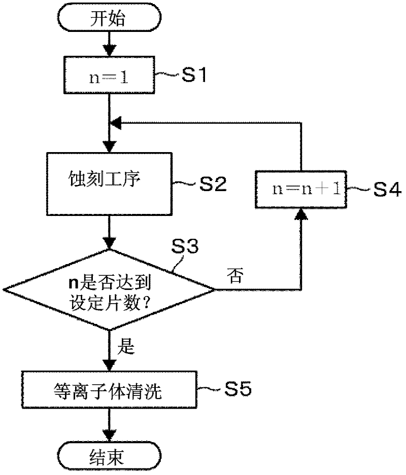
[0069] Both the surface roughness and the diameter of the island-shaped portion 91b of Example 1 were approximately equal to those of Reference Example 1, but compared with Example 1, the surface roughness of Comparative Example 1 was increased and the diameter was decreased. From this, it was confirmed that in the plasma cleaning process not using the dummy wafer, damage to the surface of the electrostatic chuck 33b can be reduced by applying a DC voltage.
Login to View More PUM
 Abstract
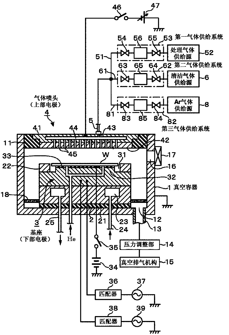
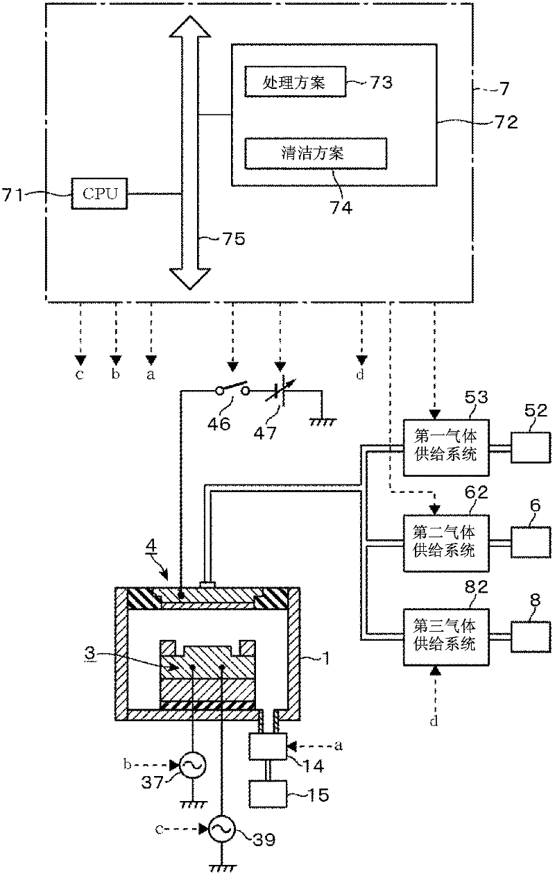
In a plasma processing apparatus for performing a plasma process on a substrate, a damage on a surface of a mounting table can be suppressed without using a dummy wafer when cleaning an inside of the plasma processing apparatus. Upon the completion of a plasma etching process, a surface of the susceptor 3 is exposed, and an inside of a vacuum chamber 1 of the plasma etching apparatus is cleaned by plasma P. Thus, reaction products A adhering to the inside of the vacuum chamber 1 are removed. Here, a DC voltage is applied to the plasma P during the cleaning process. As a result, while obtaining high-density plasma P, the ion energy can be reduced, so that the cleaning process can be performed effectively while suppressing damage on the surface of the susceptor 3.
Description
technical field [0001] The present invention relates to a technique for cleaning the inside of a vacuum container of a plasma processing device by using plasma. Background technique [0002] In the plasma treatment of the surface of a semiconductor wafer in the manufacturing process of a semiconductor device, as the number of times of treatment increases, the amount of reaction products adhering to the inner wall of the vacuum container, the mounting table, etc. increases. Since the processing environment changes when the amount of adhesion increases, the uniformity of processing between wafers may be deteriorated, and it may also be a cause of particle generation. Therefore, for example, the inside of the vacuum container is periodically cleaned by using plasma obtained by plasmating a cleaning gas. The gas uses oxygen (O 2 ) gas to incinerate the CF reaction product. In this case, in order to prevent damage to the surface of the stage, plasma cleaning is usually perform...
Claims
Login to View More Application Information
Patent Timeline
 Patent Type & AuthorityApplications(China)
IPC IPC(8): H01J37/04H01J37/305H01L21/3065B08B7/00
CPCH01J2237/022B08B7/0035H01J37/32862H01J37/32587H01J37/3288C23C16/4405H01J37/32495H05H1/46H01L21/3065H01J37/32009
Inventor村上贵宏
OwnerTOKYO ELECTRON LTD