Light emitting diode (LED) lamp panel packaging structure and method thereof

A technology of LED light board and packaging structure, applied in the direction of semiconductor devices, electrical components, circuits, etc., can solve the problems of affecting life, large chip current, current difference, etc., to achieve the effect of improving efficiency and ensuring design life

Active Publication Date: 2012-10-17
YANCHENG DONGSHAN PRECISION MANUFACTURING CO LTD
View PDF4 Cites 2 Cited by
  • Summary
  • Abstract
  • Description
  • Claims
  • Application Information

AI Technical Summary

Problems solved by technology

[0003] In the existing LED light boards containing many LED chips, the driving circuit usually provides constant current drive to both ends of the common positive and negative electrodes, in which multiple groups of LED chips are equivalent to parallel connection. Although the total current is constant, the specific Because the forward voltage value (VF) of each chip is different, the current of each channel will be slightly different, and the final result will cause some chips to have a large current and affect the overall life.

Method used


Image

  • Light emitting diode (LED) lamp panel packaging structure and method thereof
  • Light emitting diode (LED) lamp panel packaging structure and method thereof
  • Light emitting diode (LED) lamp panel packaging structure and method thereof

Examples


Embodiment Construction

[0023] Reference herein to "one embodiment" or "an embodiment" refers to a particular feature, structure or characteristic that can be included in at least one implementation of the present invention. "In one embodiment" appearing in different places in this specification does not all refer to the same embodiment, nor is it a separate or selective embodiment that is mutually exclusive with other embodiments.

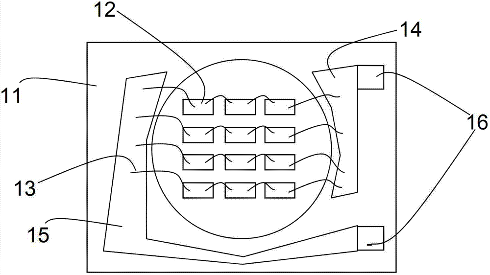
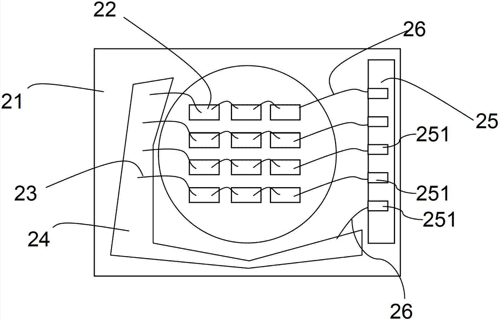
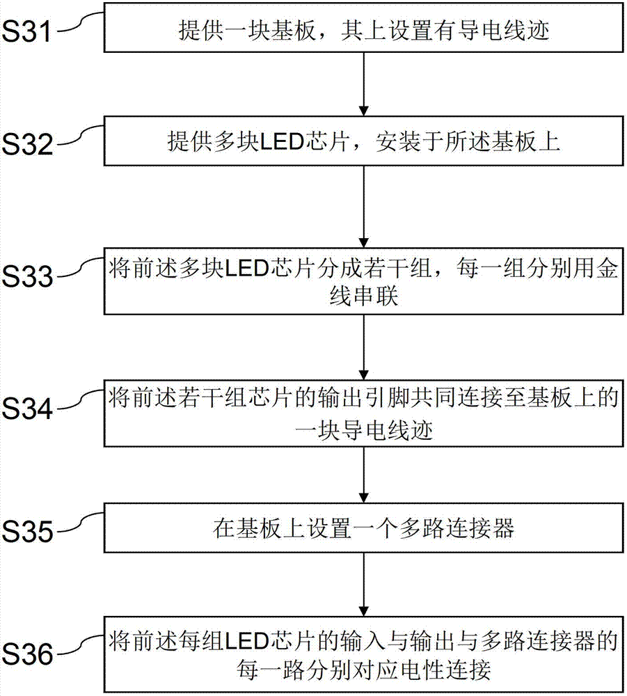
[0024] see figure 2 As shown, it shows a schematic diagram of the packaging structure of the LED light board of the present invention. Such as figure 2 As shown in , the package structure of the LED light board of the present invention includes a package substrate 21 , wherein the package substrate 21 is provided with conductive traces 24 .

[0025] A plurality of chips 22 are installed on the packaging substrate, and the plurality of chips 22 are divided into four groups, and the chips 22 in each group are connected in series through gold wires 23 .

[0026] A mult...


PUM


Abstract

The invention provides a light emitting diode (LED) lamp panel packaging structure and a driving method thereof. An LED lamp panel comprises a packaging substrate and a plurality of LED chips arranged on the packaging substrate; the chips are divided into a plurality of groups; the groups of chips are serially connected through gold wires; inputting pins of the groups of chips are jointly connected to a conductive trace; outputting pins of the groups of chips are jointly connected to another conductive trace; the conductive trace connected with the inputting pins and the conductive trace connected with the outputting pins are jointly connected to a multichannel connector, so that inputs and outputs of the groups of chips correspond to the corresponding channels of the multichannel connector, and the groups of chips are respectively driven independently.

Description

【Technical field】 [0001] The invention relates to the technical field of chip packaging, in particular to the packaging structure and method of an LED light board. 【Background technique】 [0002] In LED lighting technology, in order to achieve high brightness, one technical solution that can be adopted is to seal multiple LED chips on one packaging substrate. Such as figure 1 As shown, a plurality of LED chips 12 are divided into several groups on the packaging substrate 11, and each group of LED chips includes a plurality of LED chips 12, and these LED chips 12 are connected to each other through gold wires 13, and the anodes of the LED chips 12 of each group are connected to On a common conductive line 14, the negative poles of each group of LED chips 12 are connected to a common conductive line 15, the conductive line 14 leads to the positive pole 16 of the entire package structure, and the conductive line 15 leads to the negative pole 16 of the entire package structure,...

Claims


Application Information

Patent Timeline
Patent Type & Authority Applications(China)
IPC IPC(8): H01L25/075H01L33/62H01L33/48H01L33/00
CPCH01L2224/45144H01L2224/48091H01L2224/48137H01L2924/00014H01L2924/00
Inventor 朱德涛李秀富
Owner YANCHENG DONGSHAN PRECISION MANUFACTURING CO LTD
Why Eureka
Try Eureka