Structure for measuring bump resistance and package substrate comprising the same

A technology for measuring resistance and packaging substrates, which is applied to measuring devices, measuring electricity, measuring electrical variables, etc., can solve problems such as being unfavorable for reliability inspection at the design level, having no obvious help in reliability analysis, and being unable to observe multiple solder joints. Achieve the effect of improving reliability analysis efficiency, reducing time, and reducing the difficulty of positioning

Active Publication Date: 2012-10-24
SPRING FOUND OF NCTU
View PDF7 Cites 10 Cited by
  • Summary
  • Abstract
  • Description
  • Claims
  • Application Information

AI Technical Summary

Problems solved by technology

[0011] With this known measurement method, when it is desired to measure the resistance of n solder bumps, it is necessary to provide n auxiliary bumps, 2n voltage measurement pads, and 2n current lines
In addition, although this structure can accurately measure the change of a single solder joint, it cannot make an overall observation of multiple solder joints on the entire circuit, which is of no obvious help in reliability analysis
And because the observed structure is limited to a single solder joint, if there is a change in the microstructure of the overall structure elsewhere, the structure will not be known
In addition, because the observation is limited to a single contact point, if you want to compare different test structures, you need to produce a large number of test pieces with different structures. This method will greatly increase the cost required for testing and comparing various structural parameters, and will not be conducive to design. level reliability test

Method used


Image

  • Structure for measuring bump resistance and package substrate comprising the same
  • Structure for measuring bump resistance and package substrate comprising the same
  • Structure for measuring bump resistance and package substrate comprising the same

Examples


Embodiment 1

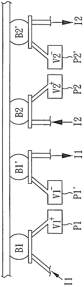
[0039]Such as Figure 4 As shown, it is a schematic connection diagram of the resistance measurement structure of the bump contact in this embodiment, including: the first to fifth solder bumps B1-B5, arranged in a line; the first connection pads C1, C3, C5; And the second connection pads C2, C4, C6; the first solder bump B1 and the second solder bump B2 are electrically connected by the first connection pad C1, and the second solder bump B2 is connected to the third solder bump B2 The bump B3 is electrically connected with the second connection pad C2, the first connection pad C1 is connected with a first voltage measurement pad P1; the second connection pad C2 is connected with an auxiliary connection pad P2', and the auxiliary connection pad P2' is connected with An auxiliary bump B2' is connected, and a second voltage measuring pad P2 is connected to the auxiliary bump B2'.

[0040] The third solder bump B3 and the fourth solder bump B4 are electrically connected by the f...

Embodiment 2

[0050] Such as Figure 5 As shown, it is a schematic diagram of the electrical connection of the resistance measurement structure of the bump contact of the packaging substrate of the present embodiment, and Figure 6 yes Figure 5 Sectional view of midline X-X'. Please also see Figure 5 and 6 , in this example, such as Figure 5 As shown, the auxiliary bumps B2', B4', the first voltage measurement pads P1, P3, and the second voltage measurement pads P2, P4 are located on the same side of the first to fifth solder bumps B1-B5. The first connection pads C1, C3, the first voltage measurement pads P1, P3, and the second voltage measurement pads P2, P4 are located on the printed circuit board 31 (such as Figure 6 shown), the second connection pads C2, C4 are located on the semiconductor chip 32 (such as Figure 6 shown) surface. The solder bumps B1-B5 are disposed between the first connection pad and the second connection pad.


PUM


Abstract

A structure for measuring bump resistance and a package substrate comprising the same are disclosed, the structure for measuring bump resistance of the present invention comprises: plural connecting bumps arranged in a row,at least one first connecting element,and at least one second connecting element,wherein the nth connecting bump and the (n+1)th connecting bump connect by the first connecting element, the (n+1)th connecting bump and the (n+2)th connecting bump connect by the second connecting element, n is an odd number of 1 or more,the first connecting element connects with a first voltage-measurement pad,the second connecting element connects with an auxiliary pad, the auxiliary pad connects with an auxiliary bump, a second voltage-measurement pad connects with the auxiliary bump.

Description

technical field [0001] The invention relates to a resistance measurement structure of a bump contact and a packaging substrate containing the structure, especially a resistance measurement structure of a bump contact combining a Kevin structure and a rosette structure and a packaging substrate containing the structure. Background technique [0002] Resistance measurement is the most basic and important one in electronic material detection. From the measured resistance, the resistivity of the material can then be deduced. When applied to the package substrate, it can test whether the connection solder bumps are defective. [0003] Among the known methods for measuring resistance, there is a kevin structure (or four point probe structure) for resistance measurement. Such as figure 1 As shown, to measure the resistance of the object under test 10, four probes 11, 12, 13, 14 are provided, wherein the probes 13, 14 provide a current path and the other two probes 11, 12 measure...

Claims


Application Information

Patent Timeline
Patent Type & Authority Applications(China)
IPC IPC(8): G01R27/08H05K1/11
CPCH01L2224/16227H01L22/00H01L2924/00013H05K3/3436G01R31/048H01L22/34H01L2224/16225H05K2203/162H05K1/0268H01L2224/131H01L24/10H01L24/16G01R31/71H01L2224/13099H01L2224/13599H01L2224/05599H01L2224/05099H01L2224/29099H01L2224/29599H01L2924/014
Inventor 陈智张元蔚
Owner SPRING FOUND OF NCTU
Why Eureka
Try Eureka