Semiconductor device and manufacturing method thereof
A technology of semiconductors and devices, which is applied in the field of semiconductor devices and their manufacturing, can solve problems such as insufficiency, and achieve the effects of low on-resistance, reduced on-resistance, and high withstand voltage
- Summary
- Abstract
- Description
- Claims
- Application Information
AI Technical Summary
Problems solved by technology
Method used
Image

Examples
no. 1 example
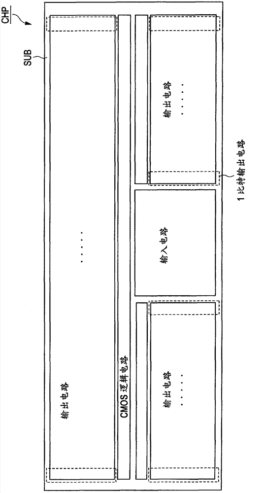
[0081] First, a semiconductor device in the state of a chip will be described in this embodiment.
[0082] see figure 1 , the semiconductor chip CHP in this embodiment has an input circuit, an output circuit, and a CMOS logic circuit. They are arranged over the main surface of the semiconductor substrate SUB.
[0083]The input circuit is a circuit for driving a CMOS (Complementary Metal Oxide Semiconductor) logic circuit and an output circuit. CMOS logic circuits are circuits used to calculate signals as they are passed from input circuits to drive output circuits, and so on. An output circuit is a circuit for outputting a signal to a load to which it is coupled (eg, a pixel of a plasma display). That is, the terminals of the output circuit are electrically coupled to the load. For example, if figure 1 The arrangement shown constitutes elements such that a collection of CMOS logic circuits is arranged above the main surface of the semiconductor substrate SUB, output cir...
no. 2 example
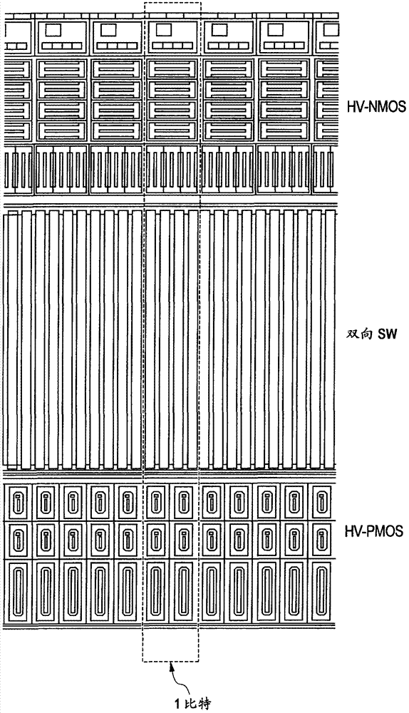
[0161] Compared with the first embodiment, this embodiment differs in the conductivity type of the epitaxial layer. will refer to Figure 31 to describe this embodiment.
[0162] with according to Figure 5 Compared with the high-voltage MOS transistor for bidirectional switching shown in the first embodiment, Figure 31 The high-voltage MOS transistor for bidirectional switching shown in is only different in that the conductivity type of its epitaxial layer NEP is n-type. That is, in this embodiment, both the epitaxial layer NEP and the well region HVNW contain n-type impurities, and the conductivity types of the epitaxial layer NEP (first impurity layer) and the well region HVNW (second impurity layer) are the same (both Contains n-type impurities).
[0163] Given the above, when combined with Figure 5 When compared with the configuration of the first embodiment shown, the Figure 31 The high voltage MOS transistor configurations of this embodiment shown in the differ...
no. 3 example
[0168] Compared with the first embodiment, this embodiment is different in the conductivity type and the like of each constituent element. will refer to Figure 32 to Figure 34 to describe this embodiment.
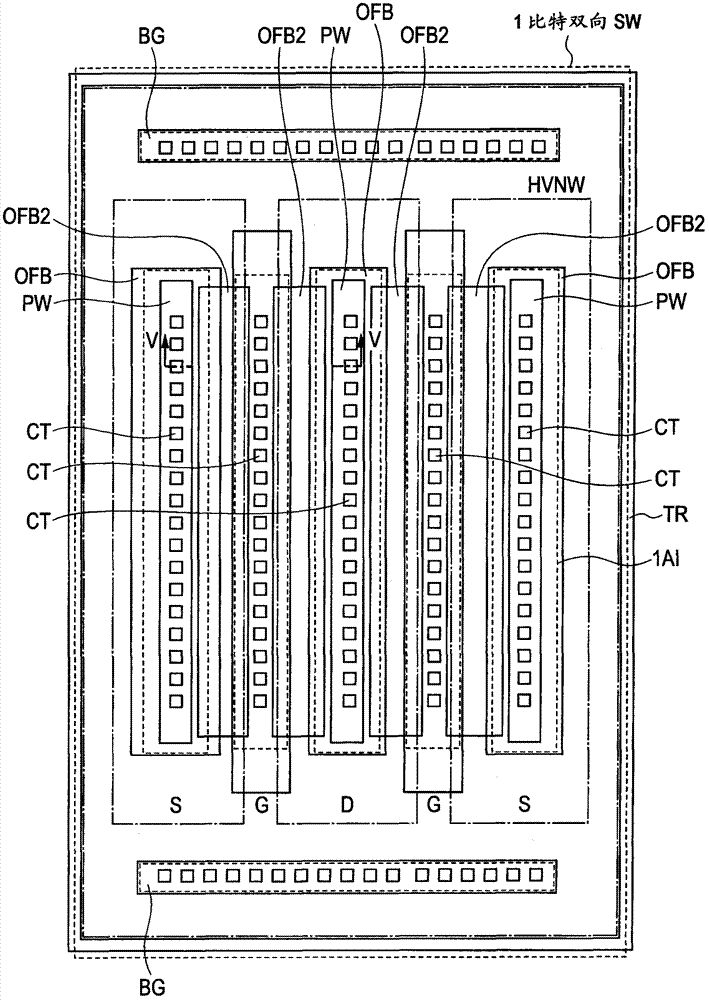
[0169] Figure 32 High-voltage MOS transistors for bi-directional switches and based on Figure 5 The high voltage transistor of the bidirectional switch of the first embodiment shown is different in that the first impurity layer (epitaxial layer NEP), the second impurity layer (high voltage well region HVPW), the third impurity layer OFP, the fourth impurity layer (diffusion layer NW), the conductivity types of the fifth impurity layer OFP2 and the contact diffusion layer NWC. That is, the high voltage well region HVPW has p-type impurities, and the diffusion layers OFP and OFP2 have n-type impurities. Preferably, the n-type impurity is, for example, the same phosphorus (P) impurity as in the first embodiment, and the p-type impurity is, for example, the same boron (B...
PUM
 Abstract
Description
Claims
Application Information
 - R&D Engineer
- R&D Manager
- IP Professional
- Industry Leading Data Capabilities
- Powerful AI technology
- Patent DNA Extraction
Browse by: Latest US Patents, China's latest patents, Technical Efficacy Thesaurus, Application Domain, Technology Topic.
© 2024 PatSnap. All rights reserved.Legal|Privacy policy|Modern Slavery Act Transparency Statement|Sitemap