Electronic device and method of making the same

A technology of electronic devices and manufacturing methods, which is applied in the direction of radiation control devices, circuits, electrical components, etc., can solve the problems of large occupation and difficulty in miniaturization, and achieve the effect of reducing volume, facilitating miniaturization, and saving the area of ​​substrates

Active Publication Date: 2015-08-05
UNIMICRON TECH CORP
View PDF6 Cites 0 Cited by
  • Summary
  • Abstract
  • Description
  • Claims
  • Application Information

AI Technical Summary

Problems solved by technology

[0007] In view of the various deficiencies of the above-mentioned prior art, the main purpose of the present invention is to provide an electronic device with a small substrate area and its manufacturing method, so as to solve the problem that the electronic device in the prior art occupies a large substrate area and is difficult to issues such as miniaturization

Method used


Image

  • Electronic device and method of making the same
  • Electronic device and method of making the same
  • Electronic device and method of making the same

Examples


Embodiment Construction

[0047] The implementation of the present invention is described below through specific specific examples, and those skilled in the art can easily understand other advantages and effects of the present invention from the content disclosed in this specification.

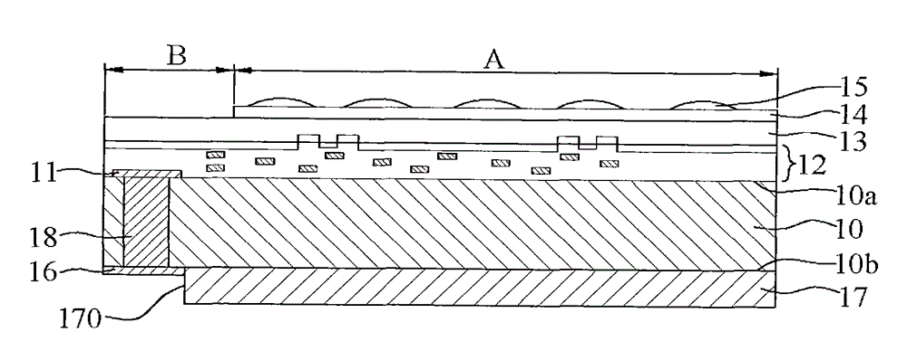
[0048] see Figures 2A to 2G , is a schematic cross-sectional view of the electronic device of the present invention and its manufacturing method, wherein, Figure 2G ’ and 2G” for Figure 2G other implementations.

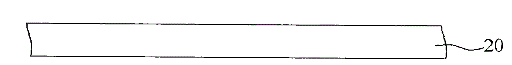
[0049] Such as Figure 2A As shown, a silicon substrate 20 is provided.

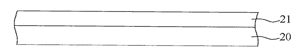
[0050] Such as Figure 2B As shown, a photodiode layer 21 is formed on the silicon substrate 20, and the material of the photodiode layer 21 can be amorphous silicon (amorphous silicon).

[0051] Such as Figure 2C As shown, a wiring layer 22 is formed on the photodiode layer 21. The wiring layer 22 includes a plurality of stacked wirings 221. The wiring layer 22 has a plurality of transfer gates adjacent to the photodiode laye...


PUM


Abstract

The invention relates to an electronic device and a manufacturing method thereof. The electronic device comprises a photoelectric diode layer, a wire distribution layer, an electric contact pad, a passivation layer, an anti-reflecting layer, a color light filter layer, a dielectric layer and a micro lens layer, wherein the photoelectric diode layer is provided with a first surface and a second surface which are opposite; the wire distribution layer is arranged on the first surface of the photoelectric diode layer; the electric contact pad is arranged on the wire distribution layer; the passivation layer is arranged on the wire distribution layer and the electric contact pad; the anti-reflecting layer is arranged on the second surface of the photoelectric diode layer; the color light filter layer is arranged on the anti-reflecting layer; the dielectric layer is arranged on the anti-reflecting layer and the color light filter layer; and the micro lens layer is arranged on the dielectric layer, and an area where the color light filter layer, the dielectric layer and the micro lens are located is an acting area, and the electric contact pad is positioned in the acting area. According to the electronic device disclosed by the invention, the electric contact pad is arranged in the acting area, and therefore the area of a substrate in a non-acting area can be saved.

Description

technical field [0001] The invention relates to an electronic device and its manufacturing method, in particular to an electronic device with a small substrate area and its manufacturing method. Background technique [0002] With the development of technology, electronic products are changing with each passing day, and the use of semiconductor technology is becoming more and more common. Now almost all electronic devices contain many electronic components or semiconductor chips inside. [0003] Generally, electronic components or semiconductor chips are formed by forming multiple layers of dielectric layers and metal layers on a silicon substrate to form an integrated circuit (IC) capable of processing electronic signals. The Complementary Metal-Oxide Semiconductor (CMOS) image sensor, which has flourished in recent years, is an electronic device built on the basis of a standard semiconductor process, which is commonly used in digital cameras or camera modules of mobile phon...

Claims


Application Information

Patent Timeline
Patent Type & Authority Patents(China)
IPC IPC(8): H01L27/146H01L23/00H01L23/488
Inventor 曾子章胡迪群
Owner UNIMICRON TECH CORP
Why Eureka
Try Eureka