Uniwafer thermoelectric modules

A single-chip, thermoelectric technology, applied in the manufacture/processing of thermoelectric device parts, circuits, thermoelectric devices, etc., can solve the problems of restricting the use of thermoelectric technology and limited applicability, and achieve the effect of improving thermoelectric merit and reducing costs

Inactive Publication Date: 2012-11-14
ALPHABET ENERGY INC
View PDF0 Cites 6 Cited by
  • Summary
  • Abstract
  • Description
  • Claims
  • Application Information

AI Technical Summary

Problems solved by technology

However, its applicability is limited due to the above considerations
with processing and assembly such as Bi 2 Te 3 The cost associated with the PbTe material often limits the use of thermoelectric technology in all but a few applications

Method used


Image

  • Uniwafer thermoelectric modules
  • Uniwafer thermoelectric modules
  • Uniwafer thermoelectric modules

Examples


Embodiment Construction

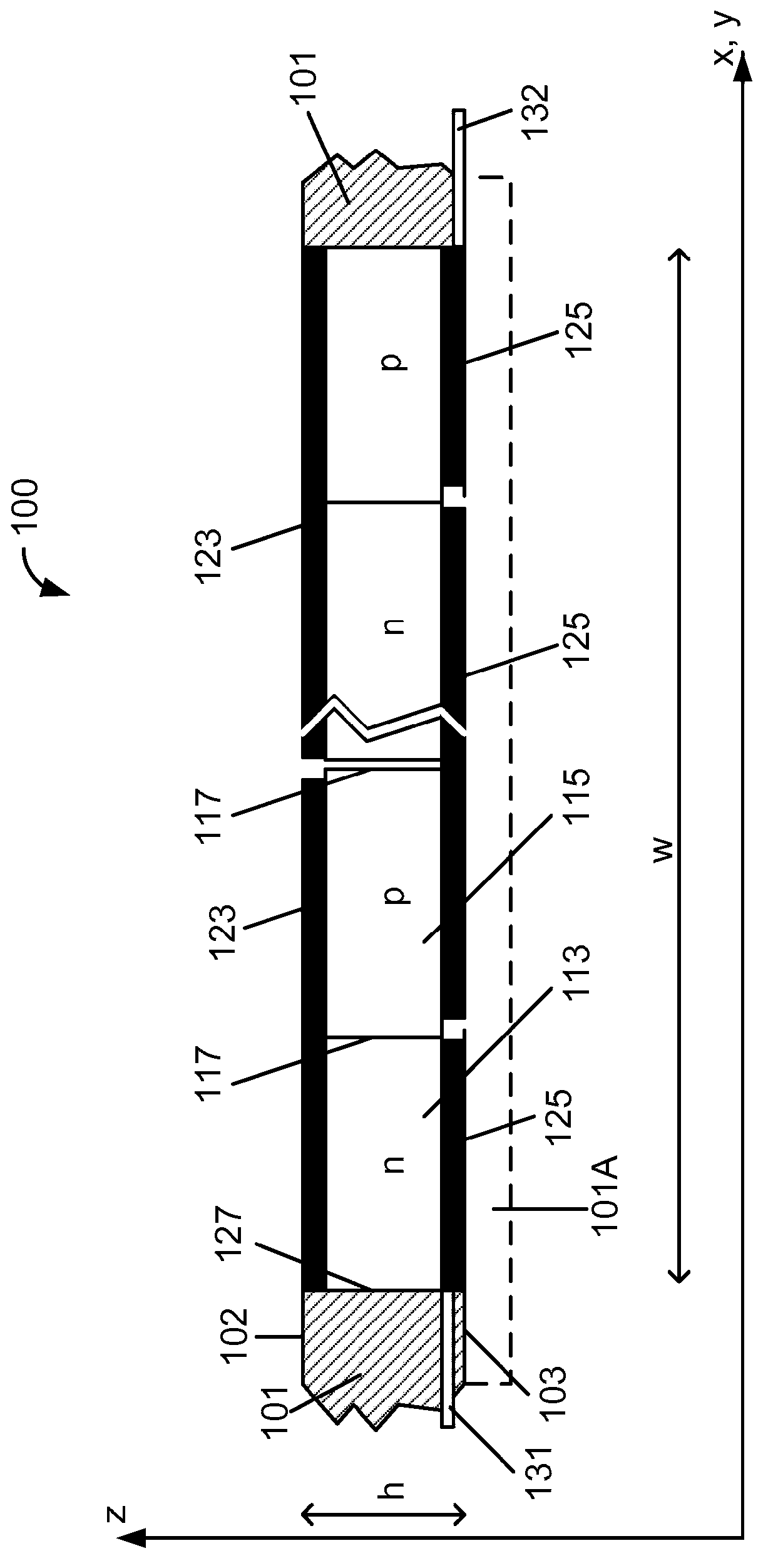
[0022] The present invention generally relates to thermoelectric devices. More particularly, the present invention provides monolithic thermoelectric devices and methods of fabrication thereof. For purposes of illustration only, embodiments of the present invention provide a method to achieve significant reductions in process complexity, number of steps, and thermoelectric module assembly costs that would require conversion of a single wafer of material into an entire thermoelectric device.

[0023] According to certain embodiments of the present invention, a method achieves a significant reduction in process complexity, number of steps, and thermoelectric module assembly costs that would require conversion of a single wafer of material into an entire thermoelectric device. For example, one such wafer on which this method can be implemented is a wafer made of silicon. Exemplary methods of implementing this basic structure according to some embodiments of the invention are out...


PUM


Abstract

A uniwafer device for thermoelectric applications includes one or more first thermoelectric elements and one or more second thermoelectric elements comprising respectively a first and second patterned portion of a substrate material. Each first / second thermoelectric element is configured to be functionalized as an n- / p-type semiconductor with a thermoelectric figure of merit ZT greater than 0.2. The second patterned portion is separated from the first patterned portion by an intermediate region functionalized partially for thermal isolation and / or partially for electric interconnecting. The one or more first thermoelectric elements and the one or more second thermoelectric elements are spatially configured to allow formation of a first contact region and a second contact region respectively connecting to each of the one or more first thermoelectric elements and / or each of the one or more second thermoelectric elements to form a continuous electric circuit.

Description

[0001] Cross References to Related Applications [0002] This application claims priority to U.S. Provisional Patent Application No. 61 / 261,174, filed November 13, 2009, entitled "THERMOELECTRIC MODULES MADE FROM A SINGLE WAFER OF MATERIAL" by inventor Matthew L. Scullin, incorporated by reference manner incorporated herein for all purposes. This application also claims priority to inventor Matthew L. Scullin's US Nonprovisional Application No. 12 / 943,134, filed November 10, 2010, which application is commonly assigned and is incorporated herein for all purposes. technical field [0003] The present invention generally relates to thermoelectric devices. More particularly, the present invention provides monolithic thermoelectric devices and methods of fabrication thereof. For purposes of illustration only, embodiments of the present invention provide methods to achieve significant reductions in process complexity, number of steps, and thermoelectric module assembly costs that...

Claims


Application Information

Patent Timeline
Patent Type & Authority Applications(China)
IPC IPC(8): H01L27/16H01L35/04
CPCH01L27/16H01L35/34H10N19/00H10N10/01
Inventor 马修·L·斯卡林
Owner ALPHABET ENERGY INC
Why Eureka
Try Eureka