Chip sorting device and chip sorting method

A technology for sorting devices and chips, which is applied in the fields of electrical components, semiconductor/solid-state device manufacturing, circuits, etc., can solve problems such as the decrease in arrangement accuracy, the length of the transmission arm 102 becomes longer, and the moving distance becomes longer, so as to improve the chip sorting accuracy , The effect of shortening chip sorting time

Inactive Publication Date: 2012-11-21
SHARP KK
View PDF2 Cites 7 Cited by
  • Summary
  • Abstract
  • Description
  • Claims
  • Application Information

AI Technical Summary

Problems solved by technology

[0005] As the size of the wafer increases and the size of the supply stage 103 of the target ring increases, the length of the transfer arm 102 of the conventional chip sorting device becomes longer, and the moving distance from the supply stage 103 to the alignme

Method used


Image

  • Chip sorting device and chip sorting method
  • Chip sorting device and chip sorting method
  • Chip sorting device and chip sorting method

Examples


Embodiment approach 1

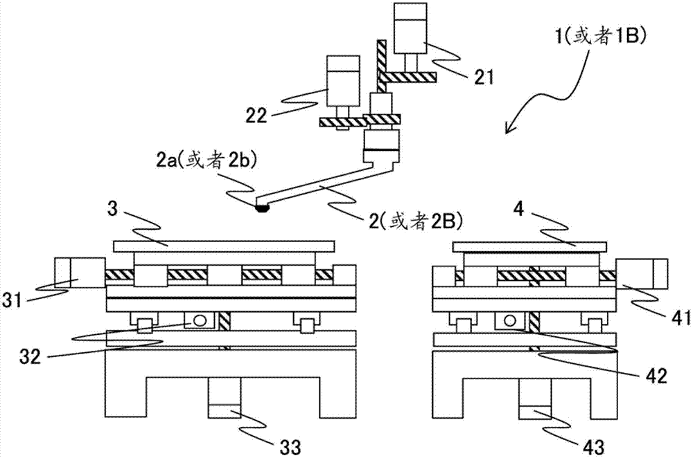
[0054] figure 1 It is a side view schematically showing an example of the configuration of the main part of the chip sorting apparatus in Embodiment 1 of the present invention.

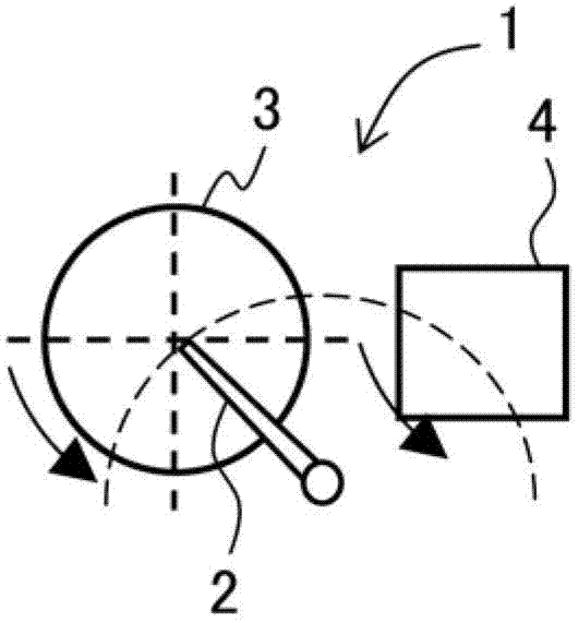
[0055] exist figure 1 Among them, in the chip sorting apparatus 1 of the first embodiment, a transfer arm 2 is provided so as to be freely rotatable and movable in the vertical direction, and the transfer arm 2 is provided with a chuck 2a at the front end portion, and the chuck 2a can One chip is sucked and held from a plurality of LED chips cut from a wafer and attached to an adhesive sheet. The vertical movement of the conveying arm 2 is performed via the rack and the pinion by the rotational drive of the motor 21 for the arm Z axis. In addition, the rotation operation of the conveyance arm 2 is performed by the rotation drive of the motor 22 for arm (theta) rotation via a gear.

[0056] In addition, in the chip sorting apparatus 1, the supply table 3 on which the ring for mounting the pluralit...

Embodiment approach 2

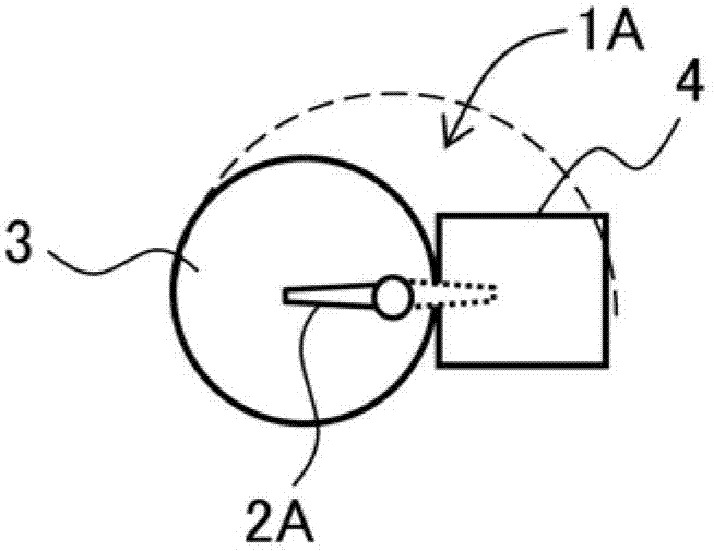
[0092] In the above-mentioned Embodiment 1, the case where the LED chips are sequentially moved from a supply table on which a plurality of LED chips are mounted on a ring to an arrangement table by one transfer arm 2, 2A, or 2B has been described. The plurality of LED chips are the plurality of LED chips cut from the wafer, but in the second embodiment, a case is described in which one transfer arm 2, 2A, or 2B is provided on the opposite side, and two transfer arms 2C pass through in total. , and sequentially move the LED chips from a supply table where a plurality of LED chips are mounted on the ring to an arrangement table, and simultaneously perform a different set of LED chips from a plurality of LED chips mounted on the ring. The operation of sequentially moving the LED chips on the supply table to one array table, wherein the plurality of LED chips are the plurality of LED chips cut from the wafer.

[0093] Figure 12 It is a plan view schematically showing the positi...


PUM


Abstract

The invention relates to a chip sorting device and a chip sorting method. Chip sorting time can be shortened and chip sorting accuracy can be improved. The chip sorting device (1) moves LED chips to an arranging work bench (4) through a conveying arm (2) from a supply workbench (3) which is carried with a plurality of LED chips being used as semiconductor chips after a wafer is cut. The length of the conveying arm (2) is at least half of the combined length of a radius of the supply workbench (3) and half of the length of a long edge of the arranging work bench (4). The supply workbench (3) moves along X-Y direction and selects a conveyed LED chip and rotates a regulated angle (90DEG), and thereby a selection area of the conveyed LED chip can be set. The supply workbench (3) and the arranging work bench (4) are respectively provided with a rotation mechanism.

Description

technical field [0001] The present invention relates to a chip sorting device that sequentially moves semiconductor chips onto an alignment table from a supply table on which a plurality of semiconductor chips that have been cut and pasted on an adhesive sheet is mounted, and chip sorting using the chip sorting device method. Background technique [0002] In this conventional chip sorting device, on the XY plane composed of two orthogonal axes, that is, the X axis and the Y axis, the cut wafers are placed on a movable table, and the wafers are cut by a CCD camera fixed on the base. To judge whether the semiconductor chip is qualified or not, the wafer is clamped by a robot or the like, and first, transferred to a fixed position correction table on the base. There are reference pressing parts in two orthogonal directions, and the positioning table fixed to the base mechanically presses and positions the chip in these two directions, and then it is clamped again by another tr...

Claims


Application Information

Patent Timeline
IPC IPC(8): H01L21/67
Inventor 佐藤哲也
Owner SHARP KK
Why Eureka
Try Eureka