Defect detecting and repairing device and method of optical sensor array panel

A sensor array and array panel technology, applied in the field of optical sensors, can solve complex, error-prone, and optical sensor array panel defects and other problems

Active Publication Date: 2012-12-19
SHANGHAI TIANMA MICRO ELECTRONICS CO LTD
View PDF7 Cites 15 Cited by
  • Summary
  • Abstract
  • Description
  • Claims
  • Application Information

AI Technical Summary

Problems solved by technology

[0012] The problem to be solved by the present invention is to provide a defect detection and repairing device and method for an optical sensor array panel, which solves the problems in the prior art such as the complex detection, positioning and repairing system of the optical sensor array panel, cumbersome detection and repairing methods, and error-proneness.

Method used


Image

  • Defect detecting and repairing device and method of optical sensor array panel
  • Defect detecting and repairing device and method of optical sensor array panel
  • Defect detecting and repairing device and method of optical sensor array panel

Examples


Embodiment 1

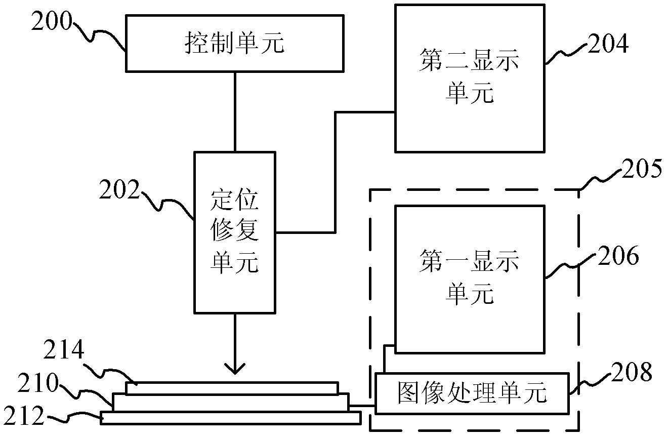
[0031] Such as figure 1 As shown, a device for detecting and repairing defects in an optical sensor array panel includes: a detection unit 210 for detecting an analog electrical signal output by an optical sensor array panel 214 placed thereon, and converting the analog electrical signal into a digital electrical signal; Process the display unit 205, convert the digital electrical signal detected by the detection unit 210 into an image signal, and convert the image signal into an image for display, and the image can feed back whether the photosensor array panel has defects; the positioning repair unit 202, The defects on the photosensor array panel 214 are located, and the located defects are repaired.

[0032] In this embodiment, the positioning repair unit 202 includes a laser source, a microscopic unit and a camera unit. The laser light produced by the laser source is irradiated on the photosensor array panel 214 placed on the detection unit 210, and the defects on the pho...

Embodiment 2

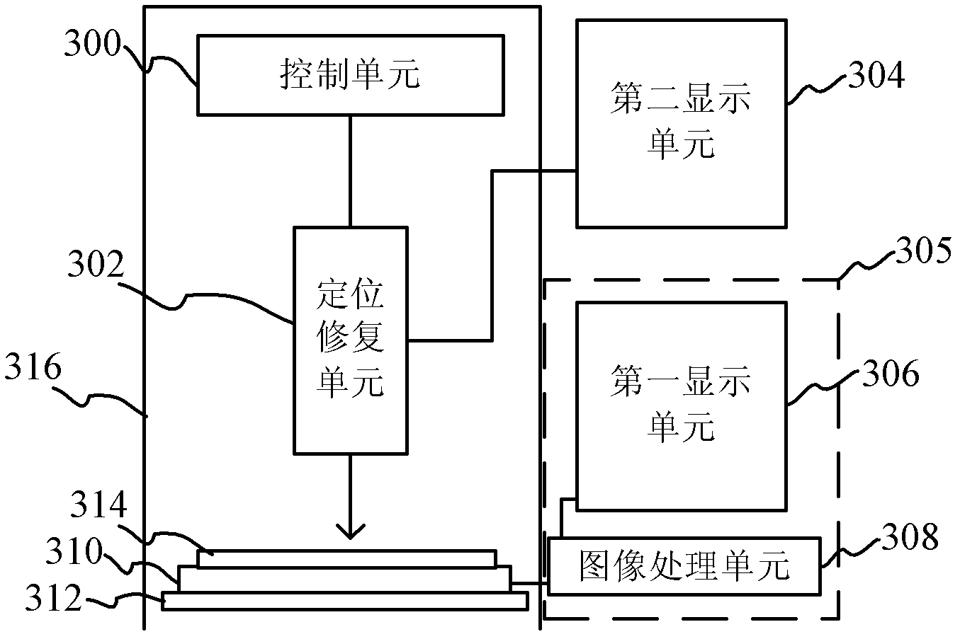
[0051] Such as image 3 As shown, a device for detecting and repairing defects of an optical sensor array panel includes: a base 312 for carrying a detection unit 310 . The detection unit 310 is configured to detect the analog electrical signal output by the light sensor array panel 314 placed thereon, and convert the analog electrical signal into a digital electrical signal. The processing and display unit 305 includes: an image processing unit 308 and a first display unit 306; the image processing unit 308 is electrically connected to the detection unit 310 to convert the digital electrical signal detected by the detection unit 310 into an image signal; The first display unit 306 is used to display the image signal obtained by the image processing unit 308 as an image. The positioning and repairing unit 302 locates defects on the photosensor array panel 314 and repairs the located defects. The second display unit 304 is electrically connected to the positioning and repairi...

Embodiment 3

[0062] Such as Figure 4 As shown, an optical sensor array panel defect detection and repairing device includes: a base 412 for carrying a detection unit 410 . The detection unit 410 is configured to detect the analog electric signal output by the light sensor array panel 414 placed thereon, and convert the electric signal into a digital electric signal. The processing display unit 405 includes: an image processing unit 408 and a first display unit 406; the image processing unit 408 is electrically connected to the detection unit 410, and is used to convert the electrical signal detected by the detection unit 410 into an image signal; the The first display unit 406 is configured to convert the image signal processed by the image processing unit 408 into an image for display. The positioning and repairing unit 402 locates defects on the photosensor array panel 414 and repairs the located defects. The second display unit 404 is electrically connected to the positioning and rep...


PUM


Abstract

The invention relates to a defect detecting and repairing device and a defect detecting and repairing method of an optical sensor array panel. The defect detecting and repairing device comprises a detection unit, a process display unit and a location repairing unit, wherein the detection unit is used for detecting an analog electric signal output by an optical sensor array panel which is arranged on the detection unit and converting the analog electric signal into a digital electric signal; the process display unit is used for receiving the digital electric signal outputted by the detection unit and converting the digital electric signal into an image to be displayed, and can judge whether the optical sensor array panel has a defect or not according to the displayed image; and the location repairing unit is used for repairing the defect after locating the defect of the optical sensor array panel. According to the defect detecting and repairing device, operations of detecting, locating and repairing the defect are finished in the same detection repair device, and the position of each pixel unit of the optical sensor array panel is determined without determining a coordinate system; furthermore a sensor pixel unit with the defect can be located after the defect is found, and the repairing effect can be determined when the defect is repaired; and therefore, the operation method is simple and convenient, is low in error rate and high in operating efficiency.

Description

technical field [0001] The invention relates to the field of optical sensors, in particular to a defect detection and repairing device and method for an optical sensor array panel. Background technique [0002] The flat-panel X-ray detector is a new type of X-ray imaging device. Because the flat-panel X-ray detector has high spatial resolution and dynamic range, and can provide fast digital image acquisition methods, the flat-panel X-ray detector has obtained a wide range of applications. [0003] The main part of the flat-panel X-ray detector is the imaging system, and the core of the imaging system is the X-ray sensor array panel. The X-ray sensor array panel is composed of a plurality of pixel units, each pixel unit includes an X-ray sensor, and the X-ray sensor is a kind of light sensor. Optical sensors accept external optical signals and convert the optical signals into electrical signals for output, mainly including photodiodes, phototransistors, photoresistors, phot...

Claims


Application Information

Patent Timeline
Patent Type & Authority Applications(China)
IPC IPC(8): G01J1/00G01T1/00
Inventor 郑礼朋
Owner SHANGHAI TIANMA MICRO ELECTRONICS CO LTD
Why Eureka
Try Eureka