Optical touch panel, manufacturing method thereof, and optical touch display panel

A technology of a touch panel and a manufacturing method, which is applied to instruments, electrical digital data processing, and input/output processes of data processing, etc. Simple process, low production cost, and the effect of improving stability

Inactive Publication Date: 2015-09-09
AU OPTRONICS CORP
View PDF5 Cites 2 Cited by
  • Summary
  • Abstract
  • Description
  • Claims
  • Application Information

AI Technical Summary

Problems solved by technology

[0004] However, since the light sensing element and the reading circuit are located on the side of the pixel array of the liquid crystal display, the area of ​​the light-transmitting region on the side of the pixel array will be compressed, resulting in a decrease in the transmittance of the display.
In this situation, the backlight module must provide higher power to achieve the same sensing signal, resulting in more power consumption. In addition, since the resolution of the light sensing element is limited by the resolution of the display, Therefore, it is difficult to increase the resolving power of the light sensing element to be greater than that of the display

Method used


Image

  • Optical touch panel, manufacturing method thereof, and optical touch display panel
  • Optical touch panel, manufacturing method thereof, and optical touch display panel
  • Optical touch panel, manufacturing method thereof, and optical touch display panel

Examples


no. 1 example

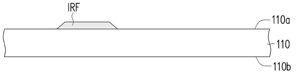
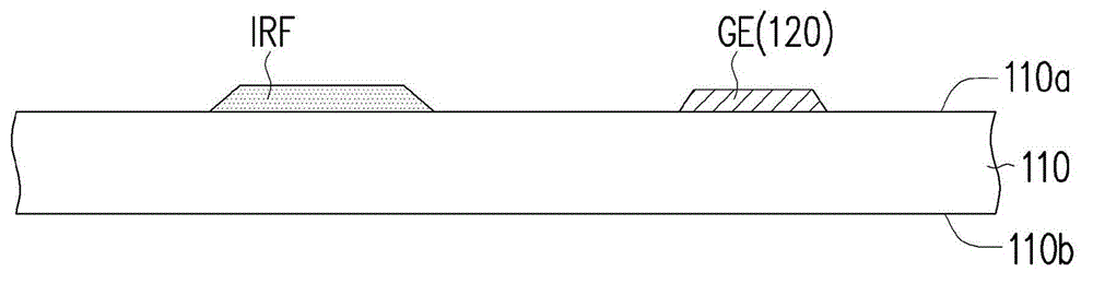
[0050] Figure 1A to Figure 1I It is a schematic cross-sectional view of the manufacturing method of the optical touch panel according to the first embodiment of the present invention. Please refer to Figure 1A Firstly, the substrate 110 is provided, wherein the substrate 110 has an inner surface 110a and an outer surface 110b, wherein the outer surface 110b faces the user. Next, an infrared filter layer IRF is formed on the inner surface 110 a of the substrate 110 . In this embodiment, the material of the infrared filter layer IRF includes germanium compound or germanium silicon compound, for example.

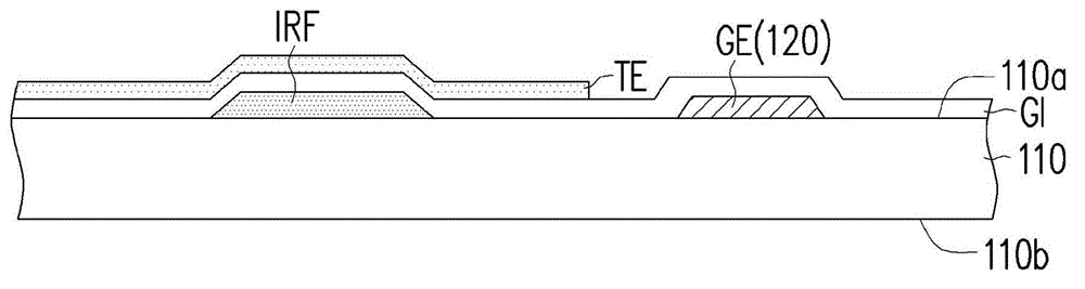
[0051] Please refer to Figure 1B, and then, a first patterned conductive layer 120 is formed on the substrate 110, the first patterned conductive layer 120 includes at least one gate GE and at least one scanning line (not marked) connected to the gate GE, wherein the gate GE and The scan lines are located on the inner surface 110 a of the substrate 110 . The material of ...

no. 2 example

[0064] Figure 2A to Figure 2I It is a schematic cross-sectional view of the manufacturing method of the optical touch panel according to the second embodiment of the present invention. Since the components of the optical touch panel of the second embodiment are the same as those described in the first embodiment, the steps and differences will be described below, and the remaining parts can refer to the first embodiment, and will not be repeated here. Please refer to Figure 2A , firstly, a substrate 110 is provided, wherein the substrate 110 has an inner surface 110a. Next, a first patterned conductive layer 120 is formed on the inner surface 110 a of the substrate 110 . The first patterned conductive layer 120 includes at least one gate GE and at least one scan line (not shown) connected to the gate GE.

[0065] Please refer to Figure 2B , and then, a first dielectric layer GI is formed on the substrate 110 to cover the gate GE and the scan line SL. Next, an infrared f...

no. 3 example

[0074] Figure 3A and Figure 3D It is a schematic cross-sectional view of the manufacturing method of the optical touch display panel according to the third embodiment of the present invention. Please refer to Figure 3A , firstly, the first substrate 110 is provided, wherein the inner surface 110a of the first substrate 110 has been formed as Figure 1H structure shown. Among them, such as Figure 1H The structure shown can be fabricated by the method described in the first embodiment or the second embodiment.

[0075] Please refer to Figure 3B , and then, a black matrix BM may be formed on the inner surface 110a of the first substrate 110 first. Then, a color filter layer CF may be formed on the inner surface 110 a of the first substrate 110 . Next, a protection layer PV2 and a transparent conductive layer TCL may be formed on the inner surface 110 a of the first substrate 110 , wherein the protection layer PV2 covers the black matrix BM and the color filter layer C...


PUM


Abstract

The invention provides an optical profile type touch panel, a manufacturing method therefor, and an optical profile type touch display panel. The optical profile type touch panel comprises an infrared light filter layer disposed on an internal surface of a substrate, a first patterning conducting layer comprises grid electrodes and scanning lines which are disposed on the internal surface of the substrate, a first dielectric layer which covers the grid electrodes and the scanning lines, a path layer disposed on the first dielectric layer and located above the grid electrodes, a second patterning conducting layer comprising source electrodes and drain electrodes which are arranged at two sides of the path layer, a transparency electrode disposed on the infrared light filter layer and electrically connected with one of the source electrode and the drain electrode, a second dielectric layer which covers the second patterning conducting layer and part of the transparency electrode, an infrared light sensing layer disposed on the transparency electrode, and a patterning shading conducting layer comprising a sensing electrode disposed on the infrared light sensing layer and a shading electrode disposed on the second dielectric layer and aligned to the path layer. The optical profile type touch panel has an excellent penetration rate and response rate,

Description

technical field [0001] The present invention relates to a touch panel, in particular to an optical touch panel and an optical touch display panel. Background technique [0002] Integrating a touch panel into a Liquid Crystal Display (LCD) not only allows users to perform convenient and fast input, but also provides interactive access functions, so it has been gradually applied to some portable electronic devices , such as a mobile phone, personal digital assistant (PDA), or laptop computer. [0003] At present, there are technologies to realize the integration of touch and display functions by embedding light sensing elements in a pixel array of a liquid crystal display. Specifically, in the touch sensing method, the sensing light source (such as infrared light) provided by the backlight module will pass through the display, and then be reflected to the light sensing element through a reflector (such as a finger). In this way, whether there is a touch event is determined b...

Claims


Application Information

Patent Timeline
Patent Type & Authority Patents(China)
IPC IPC(8): G06F3/042
Inventor 张天豪章钧范己文陈德铭卓恩宗张钧杰
Owner AU OPTRONICS CORP
Why Eureka
Try Eureka