Graphene-based S-shaped waveguide
A graphene, graphene layer technology, applied in waveguides, waveguide-type devices, circuits, etc., to achieve the effects of simple processing, strong flexibility and stability, and easy implementation
- Summary
- Abstract
- Description
- Claims
- Application Information
AI Technical Summary
Problems solved by technology
Method used
Image

Examples
Embodiment Construction
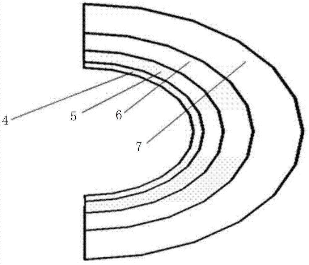
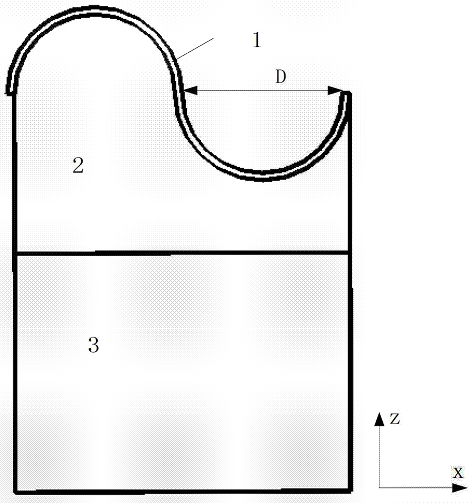
[0013] A kind of S-shaped waveguide based on graphene, comprises silicon substrate 3, is provided with silicon dioxide substrate 2 on silicon substrate 3, the upper surface of silicon dioxide substrate 2 is S-shaped undulating surface, on silicon dioxide A graphene layer 1 is laid on the substrate 2, and the chemical potential of the graphene layer 1 is 0.8eV (the corresponding carrier concentration is 4.7eV 13 cm -2 ), the shape of the graphene layer 1 matches the shape of the upper surface of the silicon dioxide substrate 2 . The chemical potential of graphene can be realized by chemical doping. In the current technology, molecular adsorption technology such as tetracyanodimethylbenzoquinone is used for doping, so that the carrier concentration of graphene can reach 1e 14 cm -2 .
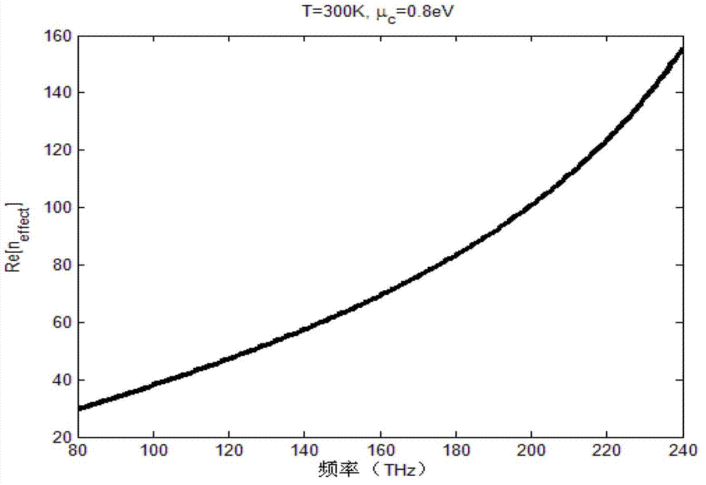
[0014] The conductivity of graphene can be expressed by the Kubo formula ("Dyadic Green's functions and guided surface waves for a surface conductivity model of graphene," J. Appl. Phys. 103(6)...
PUM
 Abstract
Description
Claims
Application Information
 - R&D Engineer
- R&D Manager
- IP Professional
- Industry Leading Data Capabilities
- Powerful AI technology
- Patent DNA Extraction
Browse by: Latest US Patents, China's latest patents, Technical Efficacy Thesaurus, Application Domain, Technology Topic.
© 2024 PatSnap. All rights reserved.Legal|Privacy policy|Modern Slavery Act Transparency Statement|Sitemap