

Display device with touch panel functionality
A technology for display devices and touch panels, which is applied to identification devices, input/output processes of data processing, optics and other directions, can solve problems such as the reduction of the aperture ratio of the display area, and achieve the effect of avoiding and suppressing the reduction of the aperture ratio.
- Summary
- Abstract
- Description
- Claims
- Application Information
AI Technical Summary
Problems solved by technology
Method used
Image

Examples
Embodiment approach 1
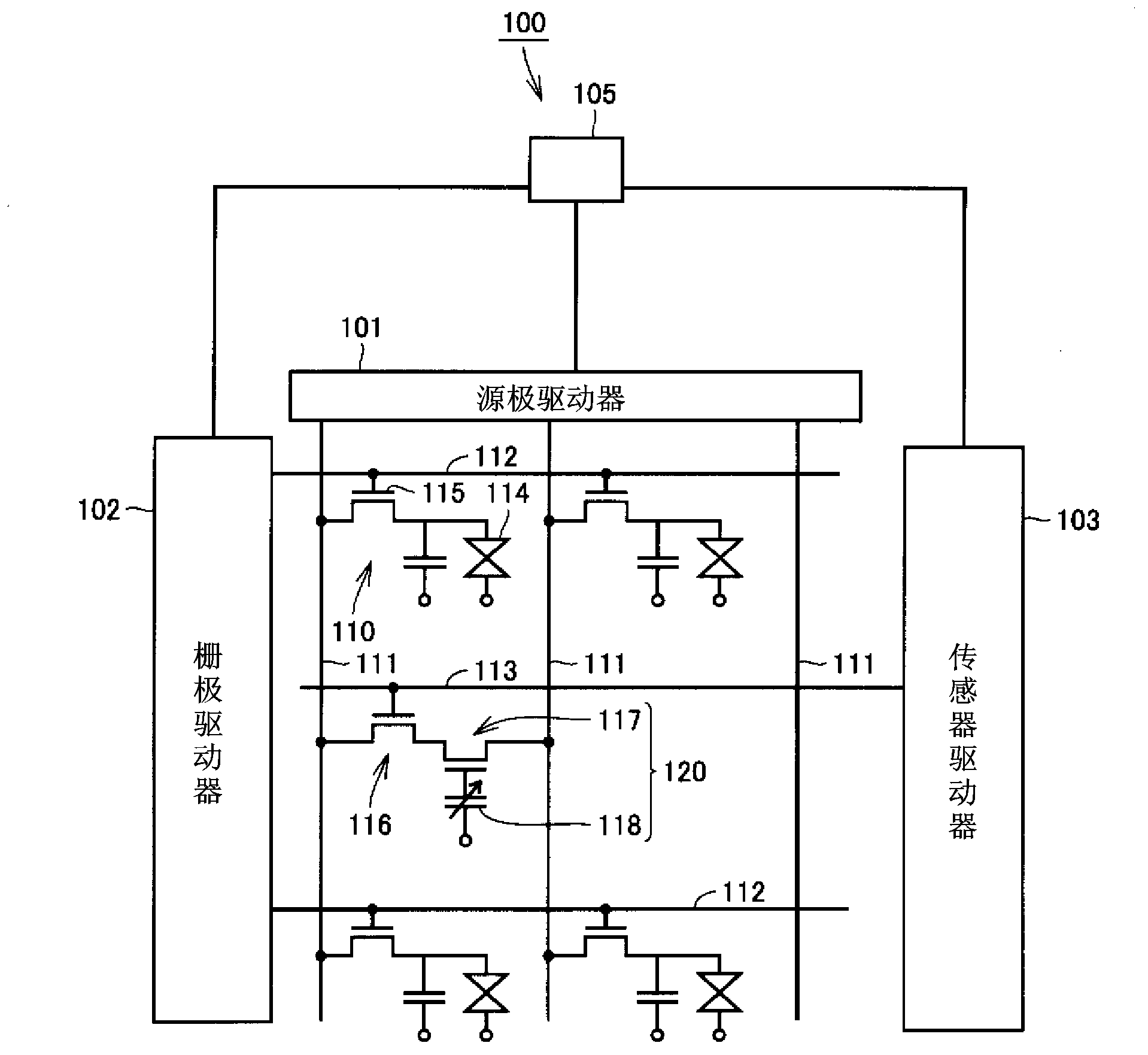
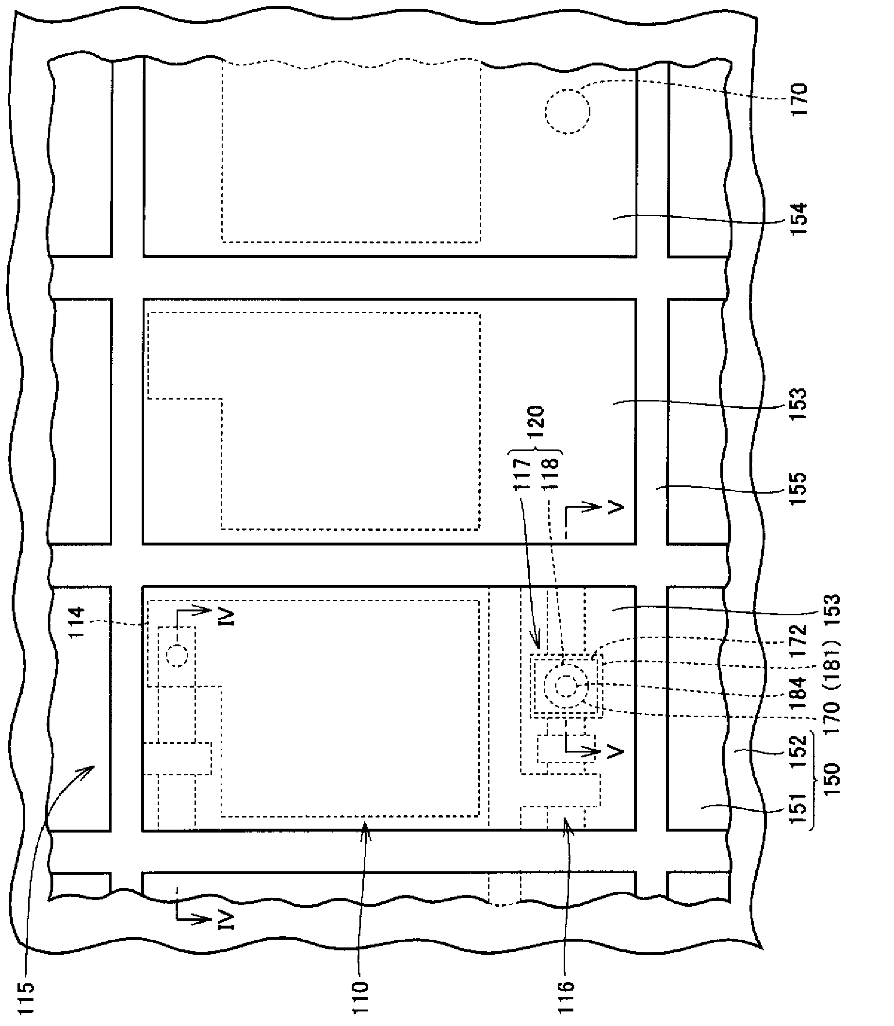
[0123] figure 1 It is a circuit diagram schematically showing a circuit diagram of the liquid crystal display device 100 of the first embodiment. As that figure 1 As shown, the liquid crystal display device 100 includes a control unit 105 and a plurality of pixels 110 arranged in an array. The pixel 110 includes a plurality of TFT (Thin Film Transistor) elements 115 and a pixel electrode 114 connected to the TFT element 115.
[0124] The liquid crystal display device 100 includes: a gate wiring 112 and a gate wiring 113 for a sensor, which extend in a first direction and are arranged at intervals in the second direction; A plurality of source wirings 111 are arranged at intervals in the direction.
[0125] Each gate wiring 112 is connected to the gate driver 102, and each source wiring 111 is connected to the source driver 101. The gate wiring 113 for a sensor is arrange|positioned between the adjacent gate wiring 112, and it extends in a 1st direction, and is formed in plural at ...
Embodiment approach 2
[0232] use Figure 22 ~ Figure 26 The pressure sensor 118 and the liquid crystal display device 100 according to Embodiment 2 of the present invention will be described.
[0233] in Figure 22 to Figure 26 In the structure shown, there is a pair of Figure 1 to Figure 21 The same or equivalent structures shown are denoted by the same reference numerals and their descriptions are omitted.
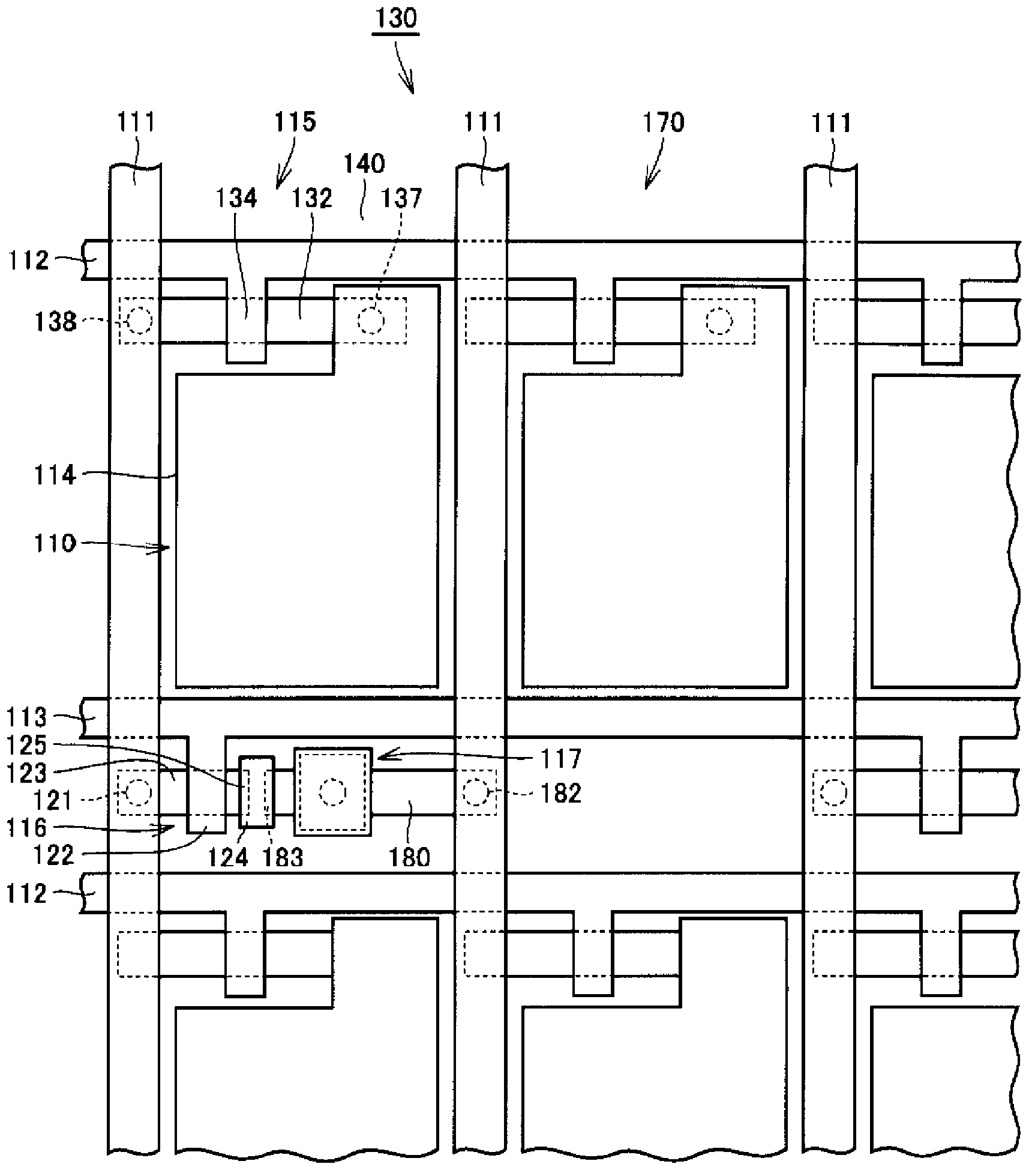
[0234] Figure 22 This is a cross-sectional view of the liquid crystal display device 100 of the second embodiment, and is a cross-sectional view showing the TFT element 115. Figure 23 It is a cross-sectional view of the liquid crystal display device 100 of the second embodiment, and is a cross-sectional view of the output element 117.
[0235] As that Figure 22 with Figure 23 As shown, the liquid crystal display device 100 includes a TFT element 115 and an output element 117, and an interlayer insulating layer 135 is formed so as to cover the TFT element 115 and the output element 117.
[0236] T...
Embodiment approach 3
[0260] use Figure 27 ~ Figure 37 The manufacturing method of the pressure sensor 118, the liquid crystal display device 100, and the liquid crystal display device 100 according to Embodiment 3 of the present invention will be described. In addition, for Figure 27 to Figure 37 The structure shown and the above Figure 1 to Figure 26 The same or equivalent structures shown may be denoted by the same reference numerals and their descriptions may be omitted.
[0261] Figure 27 This is a cross-sectional view of the liquid crystal display device 100 of the third embodiment, and is a cross-sectional view showing the TFT element 115. Figure 28 It is a cross-sectional view of the liquid crystal display device 100 of the third embodiment, and is a cross-sectional view showing the pressure sensor 118.
[0262] As that Figure 27 As shown, the liquid crystal display device 100 includes: a base layer 141 formed on the main surface of a glass substrate 140; a base layer 131 formed on the uppe...
PUM
| Property | Measurement | Unit |
|---|---|---|
| thickness | aaaaa | aaaaa |
| thickness | aaaaa | aaaaa |
| thickness | aaaaa | aaaaa |
Abstract
Description
Claims
Application Information