Active matrix substrate, display device, and short circuit defect correction method for active matrix substrate

a technology of active matrix substrate and display device, which is applied in the direction of optics, transistors, instruments, etc., can solve the problems of needing to repair display defects, new defects will occur due to wiring lines, and the wiring of tft substrates will also be severed by lasers, etc., to achieve short circuit defects, excellent display quality, and short circuit defects

Active Publication Date: 2013-12-12
SHARP KK
View PDF5 Cites 14 Cited by
  • Summary
  • Abstract
  • Description
  • Claims
  • Application Information

AI Technical Summary

Benefits of technology

[0037]According to the present invention, a slit-shaped repair hole that repairs a short circuit defect of adjacent pixel electrodes is provided, so as to straddle a storage capacitance wiring line, at at least one intersection of the edges of the plurality of the pixel electrodes and storage capacitance wiring line. Thus, if two adjacent pixel electrodes short circuit over a storage capacitance wiring line, the short circuit defect is able to be repaired using the repair holes. Specifically, laser radiation is performed to electrically isolate the short circuit defect portion, where the short circuit defect has occurred, from at least one of the two short circuited pixel electrodes. The laser radiation areas where laser radiation is performed are areas that continue to the repair holes and that do not overlap the storage capacitance wiring line. These laser radiation areas are set such that the short circuit defect portion is positioned inside the area made by the repair holes and laser radiation areas. By using the repair hole as such, the short circuit defect can be repaired without turning the entire pixel into a dark spot, and an excellent display quality can be achieved. Furthermore, by using the repair hole as such, the short circuit defect can be repaired without significantly decreasing the aperture ratio, and a high-luminance and low-power-consumption driving display device can be obtained. The short circuit defect can be repaired by merely providing the repair hole only at the intersection of the edges of the pixel electrode and the storage capacitance wiring line, and thus an active matrix substrate can be obtained that also has an excellent aperture ratio for pixels where short circuiting has not occurred.

Problems solved by technology

If two adjacent pixel electrodes short circuit with each other, for example, then the two entire pixels that have short circuited will be bright spots or defects, resulting in a need to repair these display defects.
However, if the short circuit defect has occurred in a location overlapping wiring and the like on the TFT substrate, then when the laser is used to sever the short circuit defect portion, the wiring of the TFT substrate will also be severed by the laser.
When a wiring line is severed without an auxiliary wiring line for repairing disconnection, such as a storage capacitance wiring line, new defects will occur due to the wiring line being disconnected.
Therefore, a short circuit defect repair method that radiates a laser to sever the short circuit defect portion is unable to be applied when the short circuit defect has occurred over the storage capacitance wiring line.
However, it is easily visible when two entire short circuited pixel electrodes are turned into dark spots, and the deterioration in display quality is noticeable even if repair of the short circuit defect is performed.
There is also a set standard for how many pixels in one display panel can be dark spots, and the liquid crystal display panel will be considered defective if this set number is exceeded.
Thus, there is also the risk of a reduction in yield if pixels are turned into dark spots in order to repair short circuit defects.

Method used


Image

  • Active matrix substrate, display device, and short circuit defect correction method for active matrix substrate
  • Active matrix substrate, display device, and short circuit defect correction method for active matrix substrate
  • Active matrix substrate, display device, and short circuit defect correction method for active matrix substrate

Examples


embodiment 1

Effects of Embodiment 1

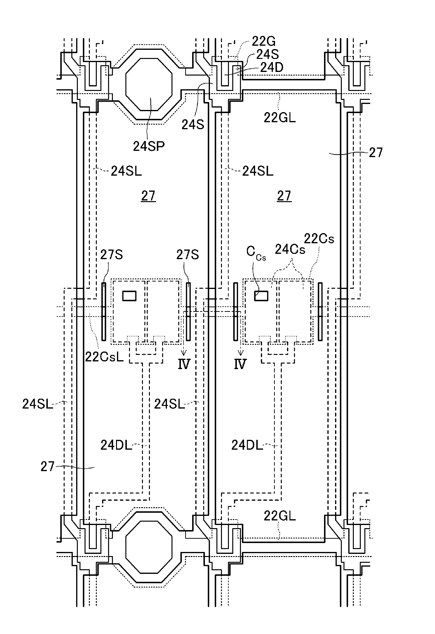
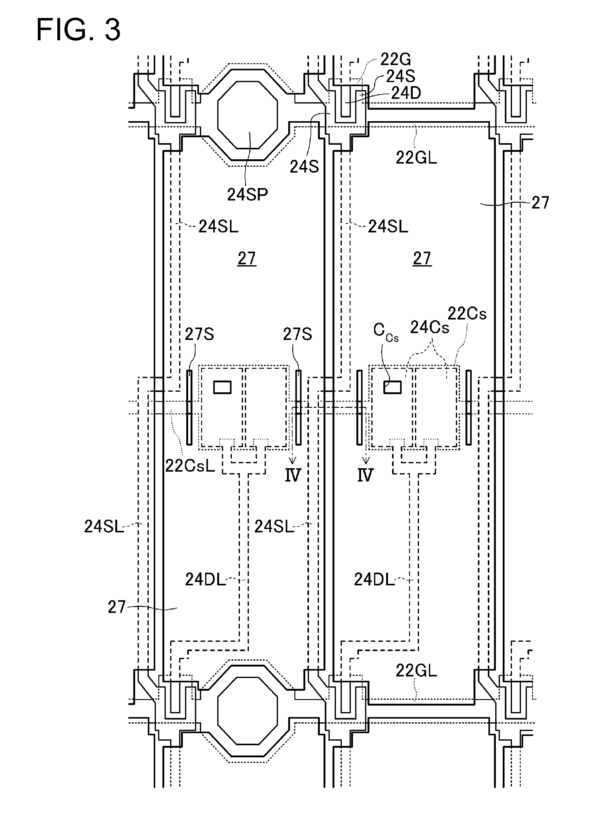
[0088]According to Embodiment 1, the area enclosed by the repair holes 27S and the laser radiation areas LS is electrically isolated from the two pixel electrodes 27S in order to stop short circuiting, and thus repair of the short circuit defect can be performed without turning the entire pixel into a dark spot. Furthermore, repair of the short circuit defect can be performed without significantly reducing the aperture ratio, and a high-luminance and low-power-consumption active matrix substrate 20 can be obtained.

modification example for embodiment 1

[0089]In Embodiment 1, as shown in FIG. 5, a short circuit occurring due to film residue left at the time of formation of the pixel electrodes 27 was described, but it is possible for short circuiting to occur among the pixel electrodes 27 for other reasons, too. As shown in FIG. 10, short circuiting will also occur among the pixel electrodes 27 due to a conductive foreign object E being present between the two pixel electrodes 27, for example. As shown in FIG. 11, the presence of the foreign object E on the periphery of the pixel electrode 27 causes film residue to be left during formation of the pixel electrodes 27, and short circuiting will occur among the pixel electrodes 27.

[0090]In Embodiment 1, each pixel electrode 27 was described as having two repair holes 27S, but as shown in FIG. 12, repair of short circuit defects can be performed even if each pixel electrode 27 has only one repair hole 27S. In this case, as shown in FIG. 13, during repair of the short circuit defect, th...

embodiment 2

Effects of Embodiment 2

[0099]According to Embodiment 2, the area enclosed by the repair holes 27S and the laser radiation areas LS is electrically isolated from the two pixel electrodes 27S in order to stop short circuiting, and thus repair of the short circuit defect can be performed without turning the entire pixel into a dark spot. Furthermore, repair of the short circuit defect can be performed without significantly reducing the aperture ratio, and a high-luminance and low-power-consumption active matrix substrate 20 can be obtained.

[0100]According to Embodiment 2, since the repair holes 27S are provided so as to not just straddle the storage capacitance wiring line 22CsL but also the source wiring line 24SL, it is possible to configure the laser radiation areas SL to be areas where the laser radiation area SL does not go across the source wiring line. Therefore, the laser radiation for stopping the short circuiting of the pixel electrodes 27 will not disconnect the source wirin...


PUM

PropertyMeasurementUnit
slit lengthaaaaaaaaaa
thicknessaaaaaaaaaa

Abstract

A slit-shaped repair hole (27S) for repairing a short circuit defect of adjacent pixel electrodes (27) is provided straddling a storage capacitance wiring line (22CsL) at at least one intersection of the edges of the plurality of the pixel electrodes (27) and the storage capacitance wiring line (22CsL).

Description

TECHNICAL FIELD[0001]The present invention relates to an active matrix substrate, a display device, and a short circuit defect repair method for an active matrix substrate. More specifically, the present invention relates to: an active matrix substrate where, when adjacent pixel electrodes short circuit over a storage capacitance wiring line, repair of a short circuit defect is possible without lowering display quality and without significantly lowering the aperture ratio; a display device provided with the active matrix substrate; and a short circuit defect repair method that repairs the short circuit defect.BACKGROUND ART[0002]Liquid crystal display devices are widely used in displays for OA devices such as TVs and personal computers, and portable devices such as cellular phones and PDAs (Personal Digital Assistant).[0003]Liquid crystal display panels generally have a structure in which a pair of transparent substrates are arranged opposing each other, with the edges thereof being...

Claims


Application Information

Patent Timeline
Patent Type & Authority Applications(United States)
IPC IPC(8): G02F1/1362H01L21/268H01L27/12
CPCG02F1/136259H01L27/1214H01L21/268G02F1/136213G02F1/1309G02F2201/506G02F2201/508G02F1/136263G02F1/136272
Inventor KANAMORI, TERUKI
Owner SHARP KK
Why Eureka
Try Eureka