Creeping-wave fault detecting probe and creeping wave fault detecting method
A creeping wave and amplitude technology, applied in the field of non-destructive testing to improve the ability to find defects
- Summary
- Abstract
- Description
- Claims
- Application Information
AI Technical Summary
Problems solved by technology
Method used
Image
Examples
Embodiment Construction
[0035] Specific embodiments of the present invention will be described in detail below in conjunction with the accompanying drawings. It should be understood that the specific embodiments described here are only used to illustrate and explain the present invention, and are not intended to limit the present invention.
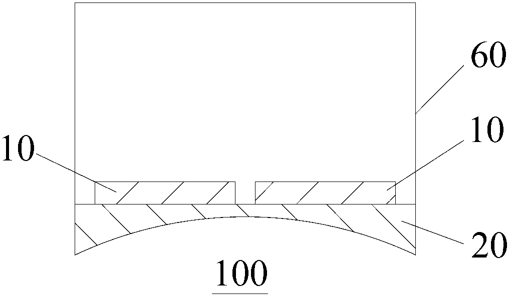
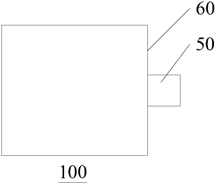
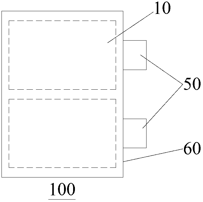
[0036] Such as Figure 1 to Figure 4 As shown, as one aspect of the present invention, a probe 100 for creeping wave flaw detection is provided. The probe 100 includes a housing 60 with an opening, a wafer 10 and a protective layer 20. The wafer 10 is arranged inside the housing 60 for protection. The layer 20 is fixedly connected to the housing 60 at the opening of the housing 60, and the housing 60 is closed. One end surface of the protective layer 20 is bonded to the wafer 10 and the protective layer 20 is fixedly connected to the wafer 10, and the other end surface It is used to conform to the surface of the object to be measured, wherein the shape of the o...
PUM
 Abstract
Description
Claims
Application Information


