Building-out circuit and testing method for testing negative bias temperature instability

A technology of negative bias temperature and instability, applied in the direction of single semiconductor device testing, etc., can solve the problems of inability to provide On-the-Fly special conditions, high cost of replacement equipment, etc., to achieve the suppression of recovery effects and accurate measurement results Effect

Active Publication Date: 2013-01-09
SEMICON MFG INT (SHANGHAI) CORP
View PDF8 Cites 19 Cited by
  • Summary
  • Abstract
  • Description
  • Claims
  • Application Information

AI Technical Summary

Problems solved by technology

However, the SMU in the old test machine cannot provide the special conditions requir

Method used


Image

  • Building-out circuit and testing method for testing negative bias temperature instability
  • Building-out circuit and testing method for testing negative bias temperature instability
  • Building-out circuit and testing method for testing negative bias temperature instability

Examples


Embodiment Construction

[0023] The principles and features of the present invention are described below in conjunction with the accompanying drawings, and the examples given are only used to explain the present invention, and are not intended to limit the scope of the present invention.

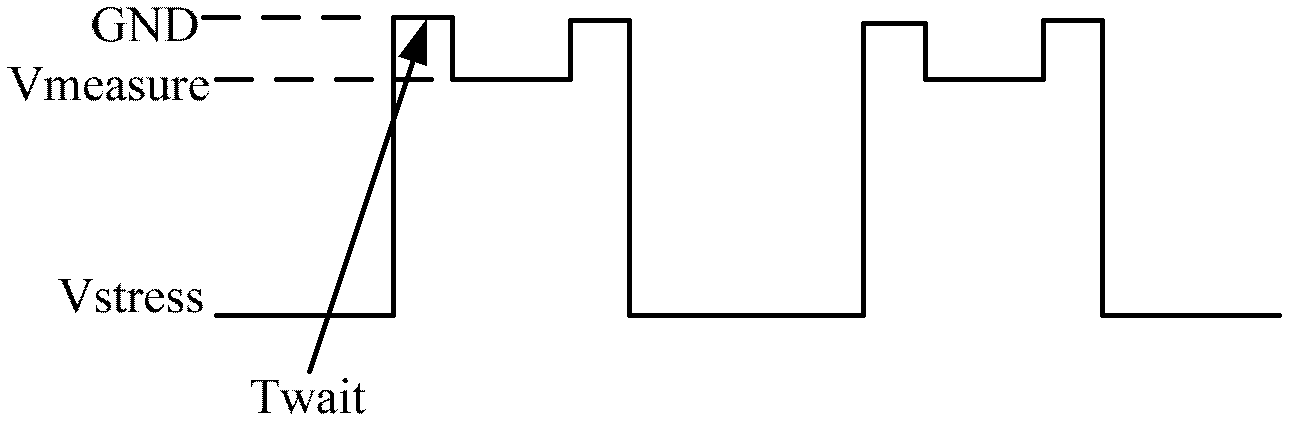
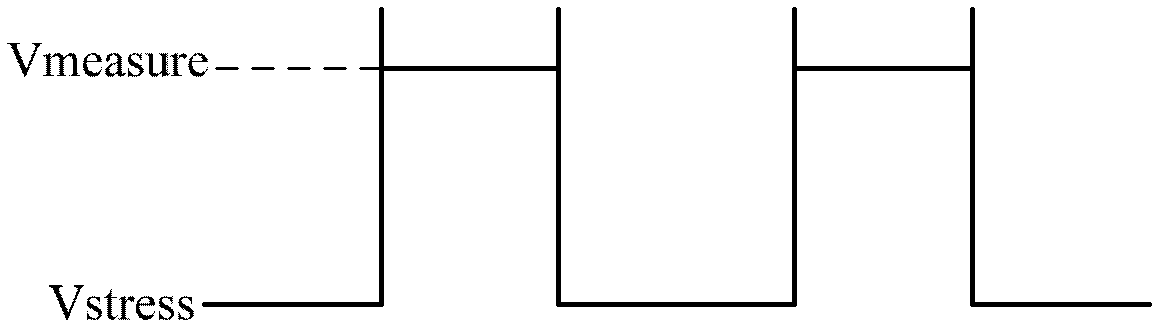
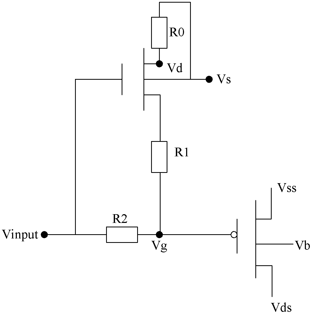
[0024] Such as image 3 A kind of NBTI test additional circuit of the present invention shown, comprises an NMOS; Wherein, the base of NMOS is electrically connected with the source of NMOS through resistance R0; The drain of NMOS is electrically connected with the PMOS gate to be tested through resistance R1; The gate of the NMOS is electrically connected to the gate of the PMOS to be tested through the resistor R2; the potential of the base of the NMOS is set to be less than 0V, and the voltage input terminal of the source-measurement unit is connected to the gate of the NMOS.

[0025] The voltage input terminal voltage of the source-measurement unit is less than or equal to 0V; the source, drain and base potentia...


PUM


Abstract

The invention provides a building-out circuit and a testing method for testing the negative bias temperature instability (NBTI). The building-out circuit is respectively connected with a source-measurement unit and a PMOS (P-channel Metal Oxide Semiconductor) to be measured; the building-out circuit comprises an NMOS (N-channel metal oxide semiconductor); a base electrode of the NMOS is electrically connected with a source electrode of the NMOS by a resistor R0; a drain electrode fo the NMOS is electrically connected with a grid electrode of the PMOS to be measured by a resistor R1; a grid electrode fo the NMOS is electrically connected with the grid electrode of the PMOS to be measured by a resistor R2; the potential of the base electrode of the NMOS is set into a value of less than 0V; and the voltage input end of the source-measurement unit is connected with the grid electrode of the NMOS. When an input voltage of the source-measurement unit is changed into 0V, due to the voltage division of the resistor R2, the voltage of the grid electrode of the PMOS to be measured is less than 0V, i.e. when the NBTI recovery effect occurs after the stress voltage is switched off, a partial pressure of the R2 is still applied to the grid electrode of the PMOS to be measured to inhibit the NBTI recovery effect in the PMOS, so that the measurement result is more accurate.

Description

technical field [0001] The invention relates to the field of semiconductor testing, in particular to a negative bias temperature instability (negative bias temperature instability, NBTI) testing additional circuit and testing method. Background technique [0002] Negative bias temperature instability (NBTI) is an important factor affecting the reliability of CMOS (Complementary Metal Oxide Semiconductor Complementary Metal Oxide Semiconductor) integrated circuits. The NBTI phenomenon has been discovered very early. For larger-sized semiconductor devices, the NBTI effect has little influence on its reliability, so it has not been paid enough attention. With the rapid development of VLSI technology to ultra-deep submicron, the device trench length L and gate oxide thickness tox continue to shrink, the voltage applied to the gate oxide layer is getting higher and higher, and the operating temperature is also increasing accordingly. Devices are becoming more and more sensitive ...

Claims


Application Information

Patent Timeline
IPC IPC(8): G01R31/26
Inventor 冯军宏
Owner SEMICON MFG INT (SHANGHAI) CORP
Why Eureka
Try Eureka