
Touch screen and manufacturing method thereof

A manufacturing method and touch screen technology, applied in the input/output process of data processing, instruments, electrical digital data processing, etc., can solve problems such as difficult to implement, difficult to implement touch screen, etc. Effect

Active Publication Date: 2013-01-09
TRULY OPTO ELECTRONICS
View PDF4 Cites 7 Cited by
  • Summary
  • Abstract
  • Description
  • Claims
  • Application Information

AI Technical Summary

Problems solved by technology

[0003] However, it is difficult to process and cut large pieces of glass after strengthening treatment, so the final step of the above-mentioned manufacturing process (that is, the step of cutting the large piece of glass into small pieces of glass) is difficult to realize, which in turn makes it difficult to use this method to make touch screens.

Method used


Image

  • Touch screen and manufacturing method thereof
  • Touch screen and manufacturing method thereof
  • Touch screen and manufacturing method thereof

Examples


Embodiment 1

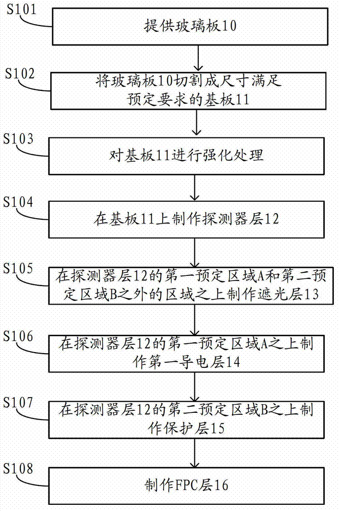
[0065] Embodiment 1 of the present invention provides a method for manufacturing a touch screen, figure 1 A flowchart showing the fabrication method, Figure 2a~2f A schematic structural diagram showing various stages of making a touch screen by using this method, reference together figure 1 and Figure 2a~2f , the production method includes:

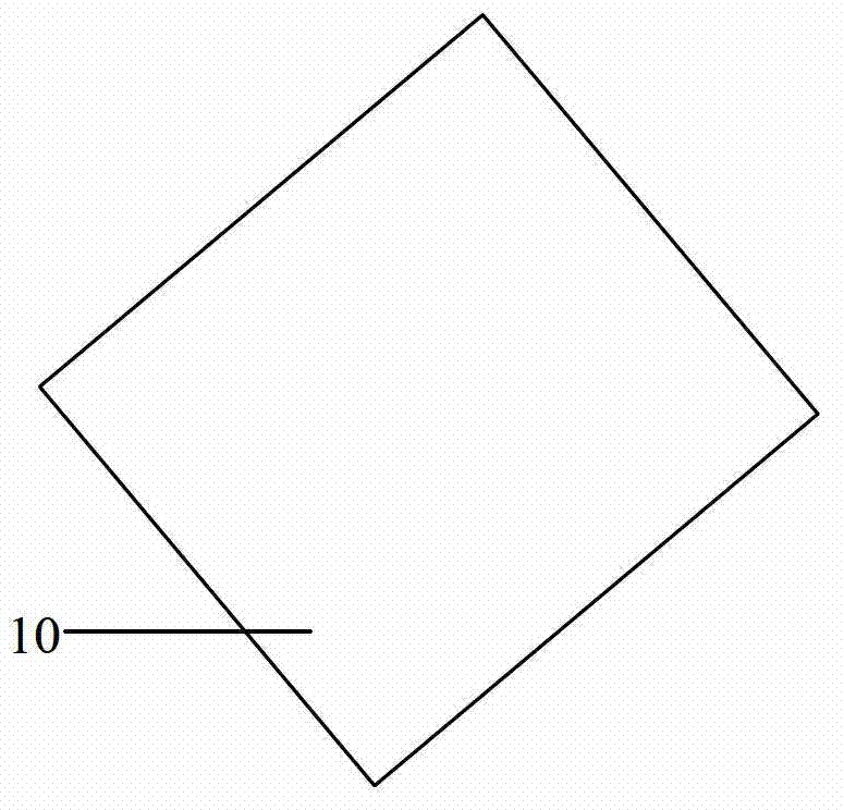
[0066] Step S101: providing a glass plate 10, such as Figure 2a shown;

[0067] The glass plate 10 in the embodiment of the present invention generally needs to have higher transparency, lower reflectivity, better thermal stability and corrosion resistance, higher mechanical strength and mechanical processing characteristics.

[0068] The glass plate in the embodiment of the present invention can be glass that can be strengthened, such as borosilicate glass without alkali ions, non-alkali aluminosilicate glass or aluminosilicate glass.

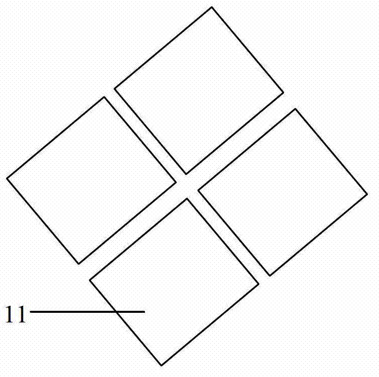
[0069] Step S102: cutting the glass plate 10 into a substrate 11 whose size meets the predeter...

Embodiment 2

[0097] Embodiment 2 of the present invention provides a method for manufacturing a touch screen, Figure 4 A flowchart showing the fabrication method, Figure 5a~5i A schematic structural diagram of various stages of manufacturing a touch screen by using this method is shown. Compared with the first embodiment of the present invention, the detector layer 12 of the touch screen provided by the second embodiment of the present invention has a multi-layer structure. Steps S401 to S403 are the same as Steps S101 to S103 in Embodiment 1. For the structural schematic diagrams of the touch screens at each stage of the manufacturing steps of Steps S403 to S403, see Figure 5a~5c (and Figure 2a~2c Corresponding), for the sake of simplification, the second embodiment of the present invention only introduces the differences from the first embodiment, and the similarities with the first embodiment can be known by referring to the corresponding description in the first embodiment, and wi...


PUM


Abstract

An embodiment of the invention provides a touch screen and a manufacturing method thereof. The manufacturing method includes providing a glass board; cutting the glass board into a substrate with the size meeting predetermined requirements; strengthening the substrate; manufacturing a detector layer on the strengthened substrate; manufacturing shading layers on regions outside a first predetermined region and a second predetermined region on the detector layer; manufacturing a first conductive layer on the first predetermined region of the detector layer; manufacturing a protective layer on the second predetermined region of the detector layer and enabling the protective layer to cover the parts of the shading layer; and manufacturing an FPC (flexible printed circuit) layer, enabling the FPC layer to cover the first conductive layer and electrically connecting the FPC layer with the detector layer via the first conductive layer. Compared with the prior art, the touch screen and the manufacturing method thereof are easy to implement.

Description

technical field [0001] The invention relates to the technical field of semiconductor manufacturing, in particular to a method for manufacturing a touch screen and a touch screen manufactured by the method. Background technique [0002] As handheld electronic devices continue to be miniaturized and thinned, touch screens used in these handheld electronic devices are required to be thinner and thinner. In order to meet this requirement, in the prior art, the touch screen is usually embedded on the glass cover. The production process of the touch screen generally adopts the following steps: first, strengthen the large piece of glass, then perform a series of operations such as printing of the light-shielding layer, making of the conductive layer, and photolithography on the strengthened glass, and finally cut the large piece of glass into small pieces of glass . [0003] However, it is difficult to process and cut the large piece of glass after strengthening treatment, so it ...

Claims


Application Information

Patent Timeline
Patent Type & Authority Applications(China)
IPC IPC(8): G06F3/041
Inventor 曹绪文吕以森李建华
Owner TRULY OPTO ELECTRONICS
Learn More